


银纳米一维复式阵列表面等离激元光谱性质
[张钦秀1, 2  , 王鹏飞
, 王鹏飞1 , 张悦1, 2 , 王婷1, 2 , 王玮1, 2 , 熊涛1, 2 , 孙诚1, 2, * ]
, 王鹏飞]
|
|


作者简介: 张钦秀, 女, 1999年生, 大连大学物理科学与技术学院硕士研究生 e-mail: zqx1197144828@163.com
纳米尺寸的贵金属在入射光的激发下能够产生表面等离激元效应, 即光在金属表面与电子发生耦合, 引起金属表面自由电子集体震荡的现象。 当自由电子的震荡频率与入射光的频率相同时, 可以引起等离激元共振, 产生独特的光谱特性。 贵金属纳米颗粒的等离激元共振效应在物理、 化学、 生物等各个领域具有广泛应用。 基于银纳米颗粒, 提出一种一维复式阵列结构, 利用时域有限差分方法研究该贵金属阵列的表面等离激元性质。 在该结构中, 以SiO2为基底, 两种不同的银纳米颗粒沿 y轴方向放置在SiO2基底的表面上, 形成一维复式阵列, 平面波入射光沿 z轴负方向垂直入射。 实验观察到, 在300~1 200 nm的波长范围内, 该复式阵列结构的表面等离激元能够被有效激发, 在其吸收光谱上有两个等离激元共振峰。 通过调节该结构纳米颗粒的尺寸、 形状和阵列周期等结构参数, 等离激元共振峰和电磁场模式均发生有规律的变化。 此外, 固定其中一个银纳米颗粒不变, 改变另一颗粒尺寸, 可以发现其吸收曲线的两个共振峰发生不同的变化, 结合电场图可以得出两个峰所对应的等离激元共振具有不同的电磁场模式。 通过改变其中一个银纳米颗粒的形状, 如四棱锥、 球体、 圆柱体和正方体, 可以发现当颗粒形状发生变化时, 两个共振峰对应的波长均不发生变化, 但是不同颗粒形状所产生的电场分布明显不同, 底面处的相对电场强度差别也很明显, 依此同样可以验证其吸收曲线存在两个不同电磁场模式的共振峰。 研究结果对基于贵金属纳米颗粒阵列结构表面等离激元器件的设计研究工作具有一定意义。
, WANG Peng-fei
Surface plasmon effects can be induced in nanoparticles of noble metals upon excitation of incident light, in which the light is coupled into free electrons, causing a collective oscillation of free electrons on the metal surface. When the oscillation frequency of free electrons is the same as that of the incident light, surface plasmon resonance may occur. The surface plasmon resonance effect of metal nanoparticles has various applications in many fields, including physics, chemistry, biology, etc. This work proposes a silver nanoparticle-based 1D composite array, and its surface plasmonic properties are investigated via the finite-difference time-domain method. In this structure, SiO2 is used as the substrate, and two silver nanoparticles are placed on the surface of the SiO2 substrate along the y-axis direction to form a 1D composite array with plane wave incident incident incident vertically along the negative z-axis direction. The results show that the surface plasmons of the 1D composite array are effectively excited in the wavelength range of 300~1 200 nm and that two plasmonic resonance peaks are revealed in the light absorption curve. The plasmonic resonances and their associated electromagnetic fields can systematically be tuned by adjusting the structural parameters of the array, including the nanoparticle size, the shape, and the period of the array. In addition, when one silver nanoparticle is fixed, and the size of the other particle is changed, it can be found that the two plasmonic resonance peaks of its absorption curve change differently. Combining the electric field diagrams, the equipartition excitonic resonance correlates to two different electromagnetic modes. By changing the shape of one of the silver nanoparticles, such as a pyramid, sphere, cylinder,orcube, it can be found that when the shape of the nanoparticle changes, the corresponding wavelength of the two plasmonic resonance peaks does not change, but the electromagnetic field distribution generated by different particle shapes is different, and the relative electromagnetic field intensity at the bottom is also significantly different. It can also be verified that the absorption curve has two different electromagnetic field modes. The results indicated in this work are significant in future research on designs of noble metal nanoparticle array-based plasmonic devices.
表面等离激元(surface plasmons, SPs)效应普遍存在于尺度较小的贵金属纳米颗粒中, 该效应通常是指某些贵金属(例如银、 金等)经过光的照射, 其表面电子与入射光发生耦合, 从而引起金属表面自由电子集体震荡的现象, 并同时伴有电磁场的产生。 等离激元共振(surface plasmons resonance, SPR)是指由于表面等离激元效应而引起的自由电子震荡的频率与入射光频率相同时, 发生在金属纳米颗粒表面的一种共振现象[1]。 通过等离激元共振效应, 可以有效地将入射光的能量进行转移, 从而达到光能利用率的提高, 增强光与物质的耦合[2]。 同时, 利用表面等离激元效应制作的生物传感器[3], 相比传统器件具有灵敏度高、 反应时间快等优点。 此外, 等离激元共振效应还可以实现拉曼散射的增强[4]、 共振峰宽泛调谐[5]等相关应用。
目前, 人们已广泛开展对贵金属等离激元共振效应的研究。 例如, Ma对金属纳米管进行仿真计算, 详细研究了纳米管的半径、 厚度、 介电函数等参数对吸收截面和局部电场的影响, 拓宽了金属纳米管在传感器和光学数据存储方面的应用[6]。 Bhardwaj提出一种镓纳米核壳结构, 改变核壳结构的尺寸, 使其折射率灵敏度提高了3%~9%, 可将其应用至生物传感器、 DNA检测等方面[7]。 Zhu提出一种金属-绝缘体-金属的结构, 经计算, 在300~2 000 nm波长范围内该结构的平均吸收率为95.21%, 最大吸收率高达99.9%, 透射率接近于零, 在太阳能电池、 光学成像等方面具有很好的潜力[8]。
在上述研究领域的基础上, 人们对由贵金属纳米颗粒构成的阵列结构的表面等离激元性质, 同样也十分关心[9]。 例如, 通过研究由铑纳米环组成的对称性破缺系统的表面等离激元性质, 依次改变光偏振的角度和破缺角的相对方向, 定量分析了该结构的散射效率, 揭示了多个等离激元共振[10]。 Nguyen设计了一种由银和硅组成的阵列结构, 通过改变不同参数来研究该结构的表面等离激元特性, 结果表明, 银纳米盘的高度对该结构的光学性质影响很小, 而银纳米盘的半径对其的影响却很大, 这一结果为生物成像和生物传感器方向提供了新思路[11]。 Chen提出一种扇形三叶片结构, 通过改变扇形金属层的厚度、 叶片半径、 阵列周期等来研究该结构的表面等离激元特性, 结果表明, 通过改变上述参数可以有效调节共振频率, 在太赫兹成像和传感应用上具有很好的潜力, 可用于提高材料的寿命[12]。
本文提出了一种基于贵金属银纳米颗粒的一维复式阵列结构, 利用时域有限差分方法, 在300~1 200 nm的波长范围内, 通过改变银纳米颗粒的尺寸、 形状、 阵列周期, 研究其表面等离激元及其光谱特性。
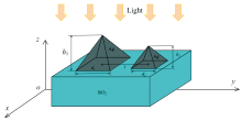
提出一种基于贵金属银纳米颗粒的一维复式阵列结构, 如图1所示, 该阵列由两种不同的银纳米颗粒沿y轴方向交替放置而成。 作为例子, 图1给出了由两种大小不同的银四棱锥(底面均为正方形)纳米颗粒所组成的一维复式阵列。 如图1所示, 四棱锥a和四棱锥b的底边边长分别用d1和d2来表示, 高分别用h1和h2来表示, 两纳米颗粒底面中心之间的间距用l来表示, 此一维复式阵列的周期为2l。 本文中, 以SiO2(n=1.46)为基底, 银纳米颗粒沿y轴方向放置在SiO2基底的表面上, 形成一维复式阵列。 平面波入射光沿z轴负方向垂直入射, 其波长在300~1 200 nm的范围之内。 时域有限差分方法(FDTD solutions, www.lumerical.com)[13]是一种对电磁场进行数值计算的重要方法之一, 其基本原理是将电磁场方程转化为差分形式, 再利用迭代算法对差分方程进行求解, 被广泛应用于研究表面等离激元领域的仿真计算中。 本文在改变纳米颗粒尺寸、 形状、 阵列周期等参数时均用到此仿真方法, 以探究该结构的等离激元特性和相应的光学性质。 在计算中, z轴方向使用完全匹配层(PML)边界条件, y轴方向则使用周期性边界条件。 计算网格大小为3 nm, 该大小的设置可以有效避免由于该模拟仿真方法所引起的误差。 银的介电常数由文献[13]中的实验数据给出, 选取当波长为0~2 μ m时的数值, 且介电常数与波长有关, 不随银纳米颗粒的尺寸和形状的变化而变化。
 | 图1 以SiO2为基底的银纳米颗粒一维复式阵列结构图 两种不同的银纳米颗粒沿y轴方向交替放置, 组成一维复式阵列; 作为例子, 图中两种纳米颗粒形状均为四棱锥(底面均为正方形), 分别用a和b标记; 其中, h1为颗粒a的高度, h2为颗粒b的高度, d1为四棱锥a的边长, d2为四棱锥b的边长, l为颗粒a和b底面中心之间的间距, 相邻颗粒间距均为l, 该一维复式阵列的周期为2l; 平面波入射光沿z轴负方向垂直入射Fig.1 Structure of a 1D composite array comprising of silver nanoparticles on SiO2 substrate In the array, two different silver nanoparticles are alternately placed along the y axis. As an example, two pyramids (the bases are both square) are demonstrated in the figure, labeled a and b, respectively. h1 is the height of particle a, h2 is the height of particle b, d1 is the length of pyramid a's base, d2 is the length of pyramid b's base, and l is the separation between the centers of the pyramids. In the array, the separation between all particles is the same, so that the period of the 1D array is 2l. A plane-wave light is normally incident along the -z axis |
阵列结构的透射率和反射率分别通过计算得出。 而后, 在同一波长下, 吸收率由透射率和反射率根据式(1)给出
式(1)中, A是吸收率(Absorption)、 T是透射率(Transmittance)、 R是反射率(Reflectivity)。
作为例子, 图2给出了一组透射率和反射率曲线图, 其中, 四棱锥a和b的尺寸分别为d1=100 nm, h1=100 nm, d2=40 nm, h2=40 nm。 利用式(1), 即可获得该参数下的吸收率曲线。
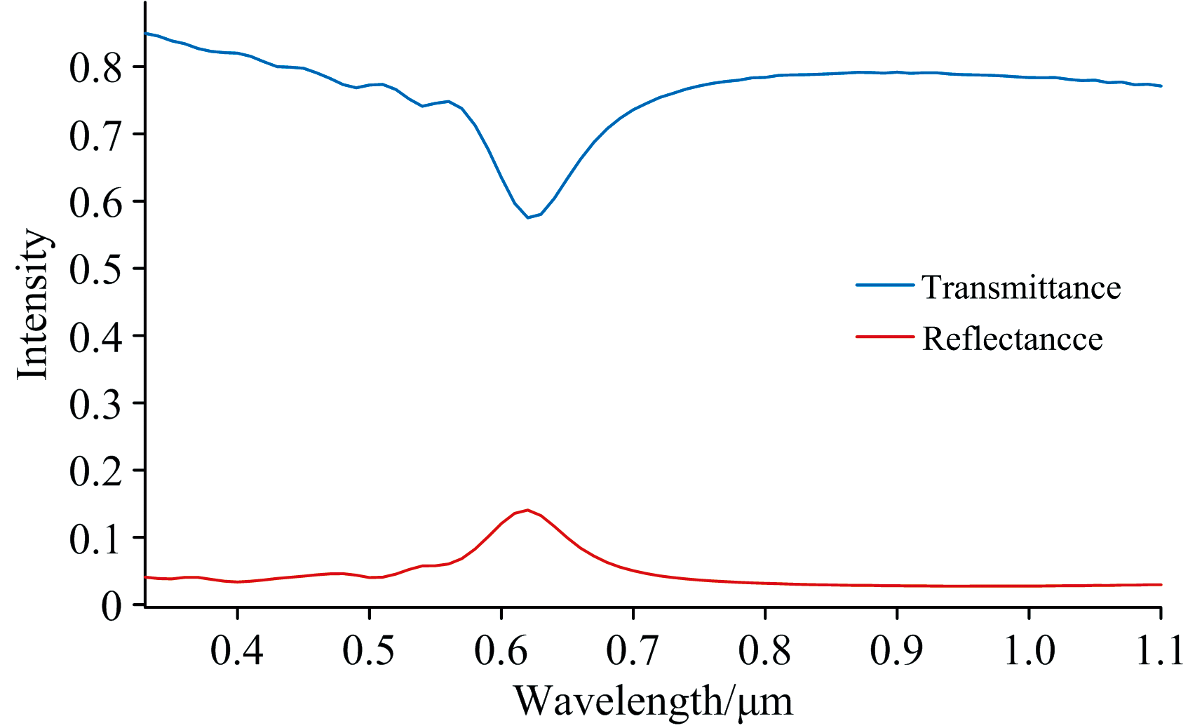 | 图2 图1所示结构的反射率和透射率曲线 四棱锥a的大小为底边边长d1=100 nm, 高h1=100 nm; 四棱锥b的大小为底边边长d2=40 nm, 高h2=40 nmFig.2 The reflectivity and transmittance curves of the structure shown in Fig.1 The size of pyramid a is d1=100 nm, and h1=100 nm. The size of pyramid b is d2=40 nm, and h2=40 nm |
利用图1所示的结构, 保持四棱锥a的尺寸不变(底边边长d1=100 nm, 高h1=100 nm), 分别进行三组研究。 一是改变四棱锥b的尺寸大小, 二是改变银纳米颗粒b的形状, 三是改变阵列周期, 分别获得该一维阵列结构的吸收曲线, 以及不同模式下的电场分布图, 从而对其性质进行分析研究。
首先, 在保持四棱锥a尺寸不变的前提下, 研究四棱锥b尺寸变化对该复式阵列光学性质的影响, 其吸收率曲线结果在图3中给出。 图3中, 四棱锥a的尺寸固定不变, 底边长为d1=100 nm, 高为h1=100 nm。 两相邻四棱锥间隔l=200 nm, 阵列周期T=400 nm, 均固定不变。 四棱锥b的底边长和高的大小保持一致, 即d2=h2, 两者同时变化, 从40 nm逐步增加至110 nm。 观察图3可知, 对于任意一条吸收率曲线, 均在不同波长处出现两个明显的峰, 表明在300~1 200 nm之间, 该一维复合阵列中的自由电子在入射光的激发下, 产生了两组等离激元共振, 方便起见, 分别用α 和β 标记。 通过测量, 这两个共振峰的波长和吸收率所对应的具体数值在表1中给出。 从表1可知, 随着四棱锥b的尺寸增加, 短波长处的α 峰对应的波长不发生改变, 均为490 nm, 而长波长处的β 峰对应的波长在630~680 nm之间逐渐增大。 此外, 两个峰所对应的吸收率峰值大小, 均随着四棱锥b尺寸的增加而逐渐增大。
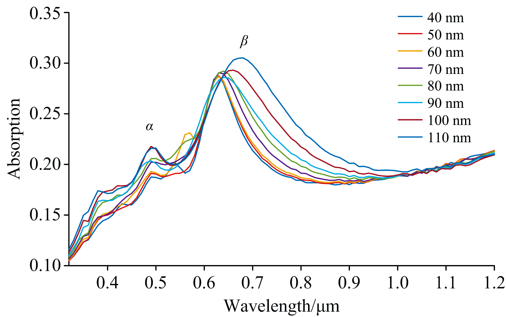 | 图3 四棱锥b不同尺寸时的吸收率曲线 四棱锥a的尺寸固定为d1=100 nm和h1=100 nm; 两相邻四棱锥间隔固定为l=200 nm, 阵列周期T=400 nm, 入射光为x偏振光。 四棱锥b的底边长和高的大小保持一样, 同时变化, 从40 nm增加至110 nmFig.3 Absorption spectra of b pyramids with varity of sizes The size of pyramid a is fixed, d1=100 nm, and h1=100 nm. The separation between two adjacent pyramids is l=200 nm, the period of the array is T=400 nm, and the incident light is x-polarized. For pyramid b, the values of the base and the height is kept the same, and they are varied simultaneously from 40 to 110 nm |
| 表1 图3中两个吸收峰(α 、 β )波长及吸收率的数值 Table 1 The values of the wavelengths and absorptions of the two peaks (α , β ) in Fig.3 |
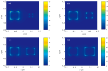
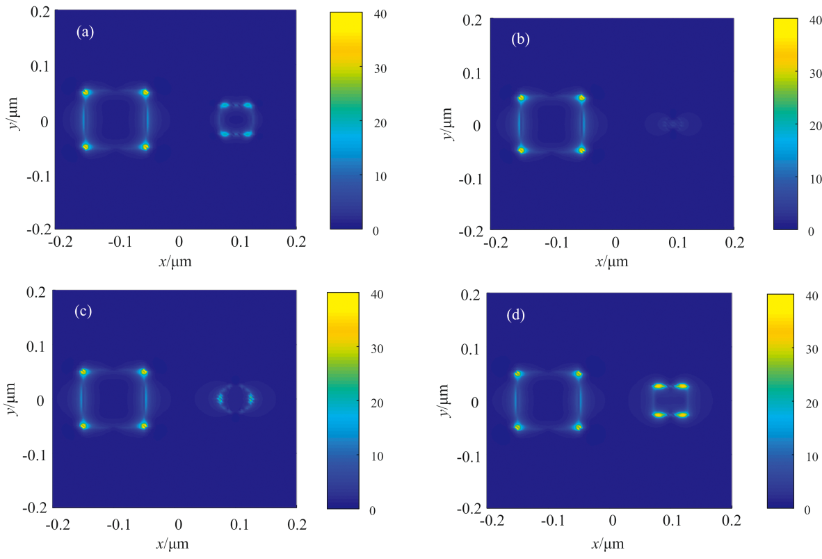
为了明确图3中两个共振峰的电磁场模式, 进一步对α 峰和β 峰所对应的电场分布进行了计算, 结果分别由图4和图5给出。 观察图4可知, α 峰波长处的电场在四棱锥a和b的底边处均有分布。 随着四棱锥b尺寸增加, 四棱锥b底边处的电场逐渐加强, 同时, 四棱锥a底边处的电场强度相对变弱。 具体比较图4(a)和(d), 图4(a)中, 四棱锥b底边处整体电场强度与四棱锥a之间的比值为0.28: 1; 然而, 随着四棱锥b尺寸增加, 在图4(d)中, 整体电场强度之比为1.24∶ 1。 说明在四棱锥b较大时, 其底边处分布的相对电场强度也较大。
 | 图4 x-y平面内, 图3中α 峰对应波长处的电场分布图 四棱锥b的底边边长和高相同, 分别为(a): 40 nm, (b): 70 nm, (c): 90 nm, (d): 110 nmFig.4 Electric field distribution in the x-y plane, at the wavelength of peak α in Fig.3 The values of the base and the height of pyramid b are the same, and they are (a): 40 nm, (b): 70 nm, (c): 90 nm, (d): 110 nm, respectively |
 | 图5 x-y平面内, 图3中β 峰对应波长处的电场分布图 四棱锥b的底边边长和高相同, 分别为(a): 40 nm, (b): 70 nm, (c): 90 nm; (d): 110 nmFig.5 Electric field distribution in the x-y plane, at the wavelength of peak β in Fig.3 The values of the base and the height of pyramid b are the same, and they are (a): 40 nm, (b): 70 nm, (c): 90 nm, (d): 110 nm, respectively |
观察图5中在β 峰波长处的电场分布, 随着四棱锥b的尺寸增加, 可以看到, 四棱锥b底边处的电场强度呈现先增加后降低的趋势, 当底边长和高均为70 nm时[图5(b)], 四棱锥b底边处整体电场最强。 此外, 通过比较四棱锥a和四棱锥b之间的相对电场强度可知, 随着四棱锥b的尺寸增加, 分布在四棱锥a底边处的相对电场强度逐渐减弱。 例如, 比较图5(a)和(d)可知, 四棱锥a和b底边处整体电场强度之比从5.5∶ 1减弱到0.72∶ 1。 综合图4和图5中给出的两组共振峰对应电场的不同变化规律, 可以看出, α 峰和β 峰所对应的等离激元共振具有不同的电磁场模式。
除了纳米颗粒的尺寸之外, 还研究了一维复式阵列中颗粒形状不同所产生的影响。 为了简便, 计算中保持银纳米颗粒a的形状为四棱锥不变(如图1中所示), 其尺寸也固定为d1=100 nm和h1=100 nm不变。 银纳米颗粒b的形状分别为四棱锥、 球体、 圆柱体和正方体, 不同形状纳米颗粒所组成一维复式阵列的吸收率曲线结果在图6中给出。 其中, 四棱锥的底边长为50 nm, 高为50 nm; 球体的直径为50 nm; 圆柱体的底边直径为50 nm, 高为50 nm; 正方体的边长为50 nm。 对于不同的颗粒形状, 从图6中均可观察到两个明显的共振峰, 类似于图3, 分别记为α 和β 。 表2给出了上述两个共振峰所对应的波长和吸收率数值。 观察表2可知, 与表1的规律不同, 当颗粒形状发生变化时, α 峰和β 峰所对应的波长均不发生变化, 分别保持为490和630 nm。 此外, 对于α 峰, 其峰值吸收率大小随形状不同而发生变化。 然而, 对于β 峰, 峰值吸收率大小几乎不因形状不同而发生改变。
 | 图6 银纳米颗粒b不同形状时的吸收率曲线 图1所示一维复式阵列中, 银纳米颗粒a的形状保持为四棱锥不变, 其尺寸固定为d1=100 nm和h1=100 nm; 两相邻纳米颗粒间隔固定为l=200 nm, 阵列周期T=400nm, 入射光为x偏振光; 纳米颗粒b的形状分别为四棱锥、 球体、 圆柱体和正方体; 其中, 四棱锥的底边长为50 nm, 高为50 nm; 球体的直径为50 nm; 圆柱体的底边直径为50 nm, 高为50 nm; 正方体的边长为50 nmFig.6 Absorption spectra of Ag nanoparticles b with different shapes The shape of Ag nanoparticle a in the 1D composite array shown in Fig.1 is kept the pyramid, and the size is fixed to d1=100 nm, and h1=100 nm. The separation between two adjacent nanoparticles is l=200 nm, the period of the array is T=400 nm, and the incident light is x-polarized. The shape of nanoparticle b is pyramid, sphere, cylinder, and cube, respectively. The values of the base and the height of the pyramid areboth 50 nm; the diameter of the sphere is 50 nm; the diameter of the base of the cylinder is 50 nm, and the height is 50 nm; the side of the cube is 50 nm |
| 表2 图6中两个吸收峰(α 、 β )波长及吸收率的数值 Table 2 The values of the wavelengths and absorptions of the two peaks (α , β ) in Fig.6 |
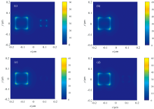
进一步地, 在图6中α 峰和β 峰对应波长处, 分别计算了纳米颗粒底边处的电场分布, 结果分别在图7和图8中给出。 通过观察图7可知, 尽管α 峰均出现在波长490 nm处, 但是不同颗粒形状所产生的电场分布明显不同, 底面处的相对电场强度差别也很明显。 例如, 图7(d)中, 正方体底面电场较强, 而图7(b)和(c)中, 球体和圆柱体底面电场较弱。 从表2中α 峰的峰值吸收率差别不大(约为0.182~0.209)可知, 由于纳米颗粒形状不同, 使得在α 峰波长处具有相似的吸收率的同时, 一维复式阵列中纳米颗粒b的具体电场分布位置明显不同。
 | 图7 x-y平面内, 图6中α 峰对应波长处的电场分布图 纳米颗粒b的形状分别为(a): 四棱锥, (b): 球体, (c): 圆柱体, (d): 正方体Fig.7 Electric field distributions in the x-y plane, at the wavelength of peak α in Fig.6 The shape of nanoparticle b is (a): pyramid, (b): sphere, (c): cylinder, (d): cube, respectively |
 | 图8 x-y平面内, 图6中β 峰对应波长处的电场分布图 纳米颗粒b的形状分别为(a): 四棱锥, (b): 球体, (c): 圆柱体, (d): 正方体Fig.8 Electric field distributions in the x-y plane, at the wavelength of peak β in Fig.6 The shape of nanoparticle b is (a): pyramid, (b): sphere, (c): cylinder, (d): cube, respectively |
观察图8, 可以明显看到, 对于四种不同的形状, 在β 峰波长处, 纳米颗粒b底面处的电场均较弱, 这说明α 峰和β 峰所对应的电场模式明显不同。 通过比较表2中两个峰对应的吸收率大小, 可以看到β 峰处峰值吸收率(约为0.289)明显大于α 峰(约为0.191), 这说明在纳米颗粒b处, β 峰的电场较多地分布在除底面以外的其他空间处, 而α 峰的电场则部分地分布在纳米颗粒的底面。
除了上述纳米颗粒的尺寸和形状外, 还研究了阵列周期对该一维复式阵列结构光学性质的影响。 如图1所示, 一维复式阵列由两个不同的四棱锥所组成, 保持两个四棱锥的尺寸不变, 分别为四棱锥a底边边长为d1=100 nm, 高为h1=100 nm, 以及四棱锥b底边边长为d2=50 nm, 高为h2=50 nm。 该一维复式阵列的周期T从400 nm逐步增大至1 000 nm, 其吸收率曲线在图9中给出。 从图9中可以发现, 随着阵列周期的变化, 上述两个共振峰α 和β 均呈现出明显的变化规律。 为了定量研究, 表3给出了α 峰和β 峰的波长和吸收率在不同周期时的数值大小。
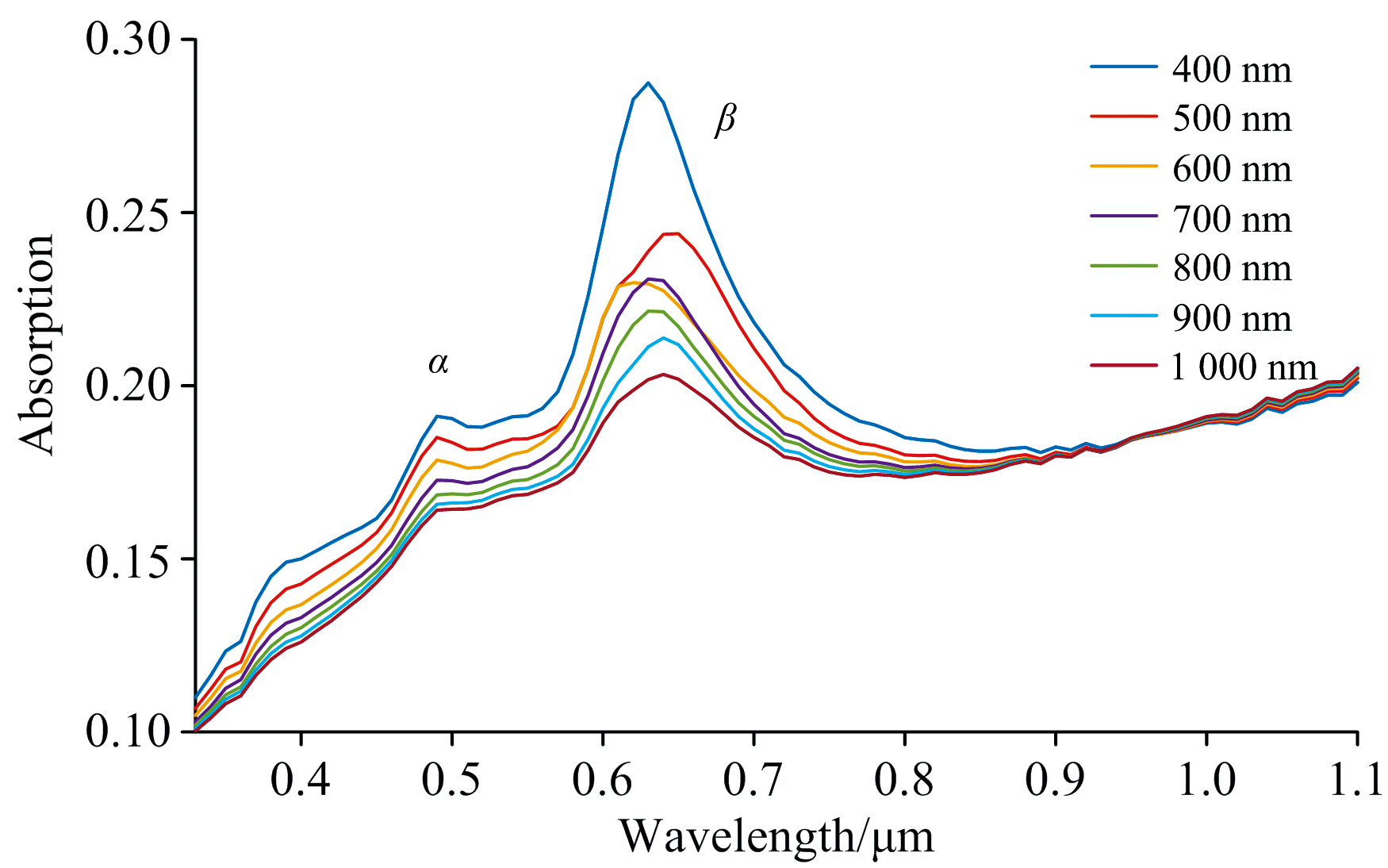 | 图9 图1所示一维复式阵列结构具有不同阵列周期时的吸收率曲线 四棱锥a和四棱锥b的尺寸分别固定为d1=100 nm和h1=100 nm, 以及d2=50 nm和高h2=50 nm; 阵列周期从400 nm增加至1 000 nmFig.9 Absorption spectra under a variety of periods for the 1D composite array shown in Fig.1 The size of pyramid a is fixed to be d1=100 nm, and h1=100 nm, the size of pyramid a is also fixed to be d2=50 nm, and h2=50 nm; The period for the array is varied from 400 to 1 000 nm |
| 表3 图9中两个吸收峰(α 、 β )波长及吸收率的数值 Table 3 The values of the wavelengths and absorptions of the two peaks (α , β ) in Fig.9 |
通过观察表3, 可以发现, 随着阵列周期的增大, α 峰和β 峰的波长均各自保持基本不变, 分别约为490和630 nm。 而峰值吸收率均随着周期的增大而减小, 具体分别为α 峰从0.19减小至0.16, β 峰从0.29减小至0.20。 这表明随着阵列周期的增大, 纳米颗粒间距的增加使得该一维复式阵列的光吸收率呈下降趋势。
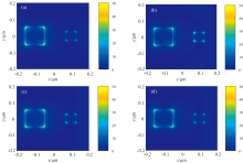
计算了图9中的两个吸收峰α 和β 在x-y平面内的电场分布, 分别由图10和图11给出。 通过观察图10和图11所示的电场分布图, 可以清晰地看到在不同阵列周期时, 纳米颗粒底边处的电场相对强度几乎没有发生明显变化。 结合表3中的峰值吸收率变化规律, 可以知道, 该一维复式阵列的周期, 可以在保持电场分布几乎不变的前提下, 用来作为有效调节光吸收率的一个结构参数。
 | 图10 x-y平面内, 图9中α 峰对应波长处的电场分布图 阵列周期分别为(a): 400 nm, (b): 600 nm, (c): 800 nm, (d): 1 000 nmFig.10 Electric field distributions in the x-y plane at the wavelength of peak α in Fig.9 The period of the array is (a): 400 nm, (b): 600 nm, (c): 800 nm, (d): 1 000 nm, respectively |
 | 图11 x-y平面内, 图9中β 峰对应波长处的电场分布图 阵列周期分别为(a): 400 nm, (b): 600 nm, (c): 800 nm, (d): 1 000 nmFig.11 Electric field distributions in the x-y plane at the wavelength of peak β in Fig.9 The period of the array is (a): 400 nm, (b): 600 nm, (c): 800 nm, (d): 1 000 nm, respectively |
提出一种基于银纳米颗粒的一维复式阵列结构, 利用时域有限差分方法, 在300~1 200 nm波段范围内, 通过改变银纳米颗粒的尺寸、 形状和阵列周期, 研究了该阵列结构的吸收光谱以及银纳米颗粒底面处的电场分布规律。 结果表明, 该一维复式阵列在300~1 200 nm波段范围内, 能够被激发出两个明显的等离激元共振峰。 其共振峰对应的波长和峰值吸收率, 均可以通过改变上述参数来有效地进行调节。 基于上述主要结果, 本文提出的一维复式阵列结构可以在300~1 200 nm波段内应用于光电调谐器件的设计和研究。
| [1] |
|
| [2] |
|
| [3] |
|
| [4] |
|
| [5] |
|
| [6] |
|
| [7] |
|
| [8] |
|
| [9] |
|
| [10] |
|
| [11] |
|
| [12] |
|
| [13] |
|