太赫兹片上系统中低温砷化镓薄膜光电导天线的研究
[张聪1, 2  , 苏波
, 苏波1, * , 张宏飞1 , 武亚雄1 , 何敬锁1 , 张存林1 ]
, 苏波, 张宏飞|
|


太赫兹时域光谱技术是一种在太赫兹频段内, 广泛应用的光谱测量技术。 这种技术可以用于许多物质的频谱分析, 对于研究化学、 半导体与生物分子等领域有着无可比拟的作用。 然而用该系统进行样品探测时, 受回波的影响频谱分辨率较低; 受太赫兹波光斑大小以及待测样品与电磁波相互作用距离长短的影响, 样品消耗量较多, 并且整个系统的占用空间较大, 这些局限性都限制了太赫兹时域光谱系统的进一步发展。 为了突破太赫兹时域光谱系统的局限性, 设计了一种将太赫兹泵浦区、 探测区和传输波导集成到一个硅片上的太赫兹片上系统, 该系统不仅能够解决上述系统的局限性, 还能够省去样品测量前的光路准直环节, 使样品的测量过程更加简便, 同时集成化的系统也很大程度上提高了太赫兹波传输的稳定性。 在太赫兹片上系统中, 泵浦区和探测区的光电导天线是由低温砷化镓和金属电极制成, 由于受到太赫兹片上系统的高度集成化和低温砷化镓晶体生长条件的限制, 如何制备出低温砷化镓半导体薄膜衬底, 并将其转移与键合, 是太赫兹片上系统研制过程中的关键环节。 首先利用分子束外延(MBE)技术制备出由半绝缘砷化镓、 砷化镓缓冲层、 砷化铝牺牲层和低温砷化镓层构成的外延片, 然后利用盐酸溶液与砷化铝和低温砷化镓反应速度差别较大的原理, 将200 nm厚的AlAs牺牲层腐蚀掉, 从而得到2 μm厚的低温砷化镓薄膜。 为了更加高效并且完整地得到低温砷化镓薄膜, 研究了盐酸溶液在不同温度和不同浓度下与AlAs牺牲层的选择性腐蚀速率的关系。 给出了低温砷化镓薄膜制备过程中盐酸的最佳体积比浓度和最佳温度, 即在73 ℃下13.57%的盐酸溶液中进行砷化铝牺牲层的腐蚀。 相比于已有工艺, 这种腐蚀方法对实验设备的要求较低并且具有较高的安全性。 最后, 将单层低温砷化镓薄膜转移键合至硅片上, 并制成光电导天线的结构。 利用飞秒激光脉冲进行激发探测到太赫兹信号。 由此说明, 低温砷化镓薄膜的获取、 转移与键合工艺能够满足芯片级太赫兹系统的制作要求, 这为太赫兹片上系统的进一步研制打下了坚实的基础。
Biography: ZHANG Cong, (1993—), master, Key Laboratory of Terahertz Optoelectronics, Ministry of Education; Beijing Key Laboratory for Terahertz Spectroscopy and Imaging; Beijing Advanced Innovation Center for Imaging Technology, Department of Physics, Capital Normal University, e-mail: 13810336797@139.com
Terahertz time-domain spectroscopy is a widely used spectrum measurement technology in terahertz frequency domain, which can be applied to the spectrum analysis of many substances, and has an incomparable role in the research of chemistry, semiconductor and biomolecule. However, the consumption of the sample is more, and the occupied space of the whole system is larger in the terahertz time-domain spectroscopy system. These limitations hinder the further development of this system. In order to overcome the limitations of the system, a terahertz on-chip system, which integrates THz generating device, detecting device and waveguide transmission device on a silicon wafer, is designed. Due to the high integration of this system and the limitation of low-temperature gallium arsenide (LT-GaAs) of photoconductive antenna growth conditions, how to fabricate the LT-GaAs semiconductor film substrate and transfer and bond it is a key step in the THz on-chip system. The epitaxial wafer consists of semi-insulating gallium arsenide, GaAs buffer layer, AlAs sacrificial layer and LT-GaAs layer. In order to obtain LT-GaAs thin film with a thickness of 2 μm more efficiently, the selective corrosion rate of HCl solution at different temperatures and different concentrations with AlAs sacrificial layer is studied. The optimum volume ratio, concentration and optimum temperature of HCl during the preparation of LT-GaAs thin film are 13.57% and 73 ℃. Compared with the existing processes, this method has higher safety performance and lower equipment requirements. Finally, the single-layer LT-GaAs thin film is transferred and bonded to a silicon wafer. Terahertz signals generated by excitation of the photoconductive antenna structure using a femtosecond laser pulse are detected, and the experiment shows that the LT-GaAs film acquisition and transfer bonding process satisfies the production requirements of the THz on-chip system and has laid a solid foundation for the development of the THz on-chip system.
Terahertz radiation is located between microwave and infrared in the far-infrared band and sits within the frequency range 0.1~10 THz and wavelength range 0.03~3 mm[1]. Terahertz time-domain spectroscopy (THz-TDS) is a typical representation of terahertz band applications and an effective coherent detection technique. This technique has been applied to the spectral analysis of a large number of substances, and plays an important role in semiconductor[2], pharmaceutical[3], and biomolecule[4] research and analysis. However, THz-TDS systems have some limitations[5]; they are far from compact, exhibit low spectral resolution and require costly sample consumption, while, terahertz spectrum extraction of water-soluble biological samples[6] is problematic owing to attenuation of the THz signal. These problems limit the development of THz-TDS systems.
The THz on-chip system not only solves the above problems but also makes the sample measurement steps more concise. In contrast with the traditional THz-TDS system, the THz on-chip system integrates the pump area of the terahertz generation, the detection area of terahertz reception and the terahertz transmission line into a single silicon wafer. Meanwhile the pumping region and the detection region adopt the photoconductive antenna structure of a gold plating electrode on the LT-GaAs semiconductor[7]. The terahertz transmission line is a microstrip line structure composed of a metal strip conductor, a dielectric layer and a gold metal ground plane[8].
The semiconductor material and electrode structure of the photoconductive antenna affect the terahertz wave characteristics. To improve the performance of the photoconductive antenna, the semiconductor material must exhibit short carrier life, large mobility and high breakdown electric field[9]. The main difference between GaAs and LT-GaAs is that the epitaxial growth temperature of LT-GaAs is 250 ℃ while the GaAs growth temperature is about 600 ℃[10]. The growth environment of LT-GaAs enables sub-picosecond carrier lifetime and higher breakdown field strength[11]. Therefore, it has high electron mobility, fast acquisition time of electrical signals, high breakdown voltage and high resistance, and is an ideal material for fabricating photoconductive antennas[12].
If the LT-GaAs is directly grown on a GaAs substrate by molecular beam epitaxy (MBE)[13], together acting as the substrate of a strip conductor, this will generate a large loss when transmitting terahertz waves. In addition, LT-GaAs crystal cannot directly grow on the dielectric layer due to lattice matching, which is required for crystal growth. It has been reported in literature that LT-GaAs film can be obtained using this structure of epitaxial wafers, which composed of Ga0.7Al0.3As, LT-GaAs, Ga0.7Al0.3As, AlAs sacrificial layers, GaAs buffer layers and GaAs substrate[14]. Here, the AlAs sacrificial layer is corroded using HF solution[15]. However, this method is not without difficulties. HF solution is both highly corrosive and highly toxic[16]. In addition, the photoconductive antenna substrate containing a 50nm-thick Ga0.7Al0.3As layer results in poor coupling efficiency of the THz wave into the microstrip line.
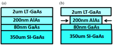
In this work, the epitaxial wafer structure consists of LT-GaAs, AlAs sacrificial layer, GaAs buffer layer and SI-GaAs substrate, as shown in Fig.1(a). The AlAs sacrificial layer is corroded to obtain a single LT-GaAs film as shown in Fig.1(b). The growth of the epitaxial wafer is carried out by MBE epitaxial equipment and the substrate is a 2-inch SI-GaAs[17]. The deposition rate of the materials is less than 1 000 nm· h-1, ensuring that the deposition quality and deposition rate can be precisely controlled. To improve the crystal growth quality, a GaAs buffer layer of 80 nm thickness is first grown at a temperature of 580 ℃, and then a 200-nm-thick AlAs sacrificial layer is lattice-matched epitaxially grown at a temperature of 550 ℃, followed by the growth of a 2-μ m-thick GaAs layer at low temperature. The growth temperature 250 ℃ is used for LT-GaAs followed by an annealing temperature of 550 ℃ for 15 minutes. The lattice constant of GaAs is close to that of AlAs and does not cause serious lattice mismatch.
 | Fig.1 LT-GaAs epitaxial wafer (a) Epitaxial wafer structure (b) Selective corrosion diagram |
For safety, the selective corrosion of LT-GaAs epitaxial wafers is carried out by using HCl solution instead of HF solution. HCl solution is a mix of 38% concentrated HCl with deionized water, and the mass fraction is obtained after calculation. Experimental result shows that the higher the mass fraction of HCl is, the faster the sacrificial layer will erode, but the reaction rates of HCl and LT-GaAs film also increase, so it is not suitable to acquire single-layer LT-GaAs film. Therefore, for finding appropriate HCl solution, the following research has been done.
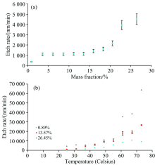
A 2-inch epitaxial film was separated into 2× 2 mm blocks, cleaned with alcohol and placed in sealed test tubes filled with prepared HCl solution of different mass fraction ranging from 0.89% to 26.45%. The corroded depth of the AlAs sacrificial layer was measured using an optical microscope and the corrosion rate was calculated according to corrosion time. For the experimental statistics, the corrosion rate is the average of six results. Fig.2 (a) shows the relationship between corrosion rate of AlAs and HCl mass fraction at room temperature. The corrosion rate of the AlAs sacrificial layer increases little in the mass fraction range 3.54% to 13.57%, and it has significantly improved above 15.94%.
 | Fig.2 Corrosion rate image (a) Relationship between the corrosion rate of AlAs and HCl mass fraction at room temperature; (b) Relationship between corrosion rate and temperature and concentration of HCl solution |
Next, the corrosion rate as a function of both temperature and concentration of HCl solution was examined. A DF-101S heated thermostatic magnetic stirrer (Beijing Kewei Yongxing Instrument Co. Ltd.) ensures temperature homogeneity. According to the relationship between the corrosion rate and concentration at normal temperature, the maximum, minimum, and intermediate concentrations of HCl solution were selected for investigation. The HCl solution with an intermediate concentration of 13.57% was chosen because the corrosion rate changes most slowly during the selective corroding of the epitaxial wafers with HCl solutions at concentrations of 3.54% to 13.57%, and the 13.57% HCl solution corrosion rate was maximum in this concentration range. To restrict volatilization of HCl during the heating process, the HCl solution occupies 90% of the space of the entire closed tube and the heating temperature was only from 25 ℃ to 73 ℃.
Fig.2(b) shows the relationship between corrosion rate and temperature and concentration of HCl solution. In general, an increase in temperature results in an increase in corrosion rate. A marked difference is observed in the rate of increase of corrosion rate for the HCl solution with mass fraction of 13.57% and 26.45%. Here, the former exhibits a linear increase in corrosion rate as a function of temperature, while the latter exhibits an exponential increase. The corrosion rate of the 0.89% HCl solution evolves somewhat differently. When the temperature reaches 73 ℃, the corrosion rate begins to decrease. The reason for this phenomenon is that the mass fraction of HCl solution decreases during heating due to the evaporation of HCl. At high concentrations of HCl in solution this evaporation does not significantly affect the HCl mass fraction.
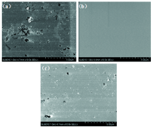
Fig.3 shows scanning electron microscope (SEM) images of LT-GaAs films selectively corroded by 0.89%, 13.57% and 26.45% mass fractions of HCl solution. Both the surfaces of the LT-GaAs thin film obtained by selective corroding with HCl solution with mass fraction of 0.89% and 26.45% are poor quality. Whereas it was found that a 13.57% HCl solution produced repeatable, good quality surfaces.
 | Fig.3 Microscopic morphologies of corroded LT-GaAs films (a) 0.89% (b) 13.57% (c) 26.45% HCl solution |
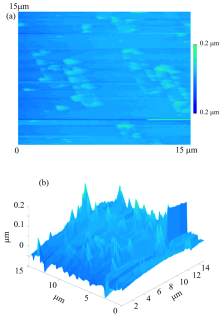
Based on the above experimental results, a 13.57% HCl solution occupying 90% of the volume of the test tube and placed in a 73 ℃ temperature water bath was used for selectively corroding the epitaxial wafer to efficiently obtain high quality LT-GaAs thin films. Then, after cleaning using deionized water and then alcohol, the prepared LT-GaAs thin film is placed on a silicon wafer. The alcohol is driven off by a slow flow of air (N2). Finally, the LT-GaAs film is bonded to the silicon wafer by the van der Waals force[18, 19]. Fig.4(a) and (b) are a two-dimensional and a three-dimensional image of the transferred and bonded LT-GaAs film, respectively, which are taken by an atomic force microscope (AFM), and the scanning area is 15 μ m× 15 μ m[20].
 | Fig.4 Scanning diagram of LT-GaAs thin film after transfer bonding(a): Two-dimensional image; (b): Three-dimensional image |
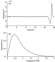
To demonstrate whether the flatness of the film after transfer bonding is compatible with the requirements of the THz on-chip system, the following experiment is performed. At first, the silicon wafer bonded with the LT-GaAs film was made into a photoconductive antenna structure by means of photolithography, vacuum evaporation and the like. Then, the two electrodes of the photoconductive antenna were connected to the wires. Finally, the prepared photoconductive antenna was examined using a terahertz time-domain spectroscopy system based on asynchronous sampling. Fig.5 is terahertz time-domain and frequency domain spectra generated by the antenna, respectively. The generation of the terahertz signal proves that the single-layer LT-GaAs film preparation, transfer and bonding processes are successful, and can meet the production requirements of the THz on-chip system.
 | Fig.5 Terahertz signal generated by antenna(a): Time domain spectrum; (b): Frequency domain spectrum |
In summary, using the molecular beam epitaxy, we have produced a new epitaxial wafer structure, which is comprised of LT-GaAs, AlAs sacrificial layer, GaAs buffer layer and a SI-GaAs substrate. A 13.57% HCl solution in deionized water at 73 ℃ is shown to obtain high quality LT-GaAs thin films. In addition, we have successfully completed the transfer and bonding process of single layer LT-GaAs films fabricating a photoconductive antenna. Compared with existing technology, the method makes the transfer and bonding process more convenient and concise. Finally, the antenna is able to meet the needs of a post-production THz on-chip system and lays a solid foundation for the development of a whole THz on-chip system.
The authors have declared that no competing interests exist.
| [1] |
|
| [2] |
|
| [3] |
|
| [4] |
|
| [5] |
|
| [6] |
|
| [7] |
|
| [8] |
|
| [9] |
|
| [10] |
|
| [11] |
|
| [12] |
|
| [13] |
|
| [14] |
|
| [15] |
|
| [16] |
|
| [17] |
|
| [18] |
|
| [19] |
|
| [20] |
|