


Structural, Optical and Electrochromic Properties of WO3 Thin Films Prepared by Chemical Spray Pyrolysis Versus Spin Coating Technique
引用本文
S. Morkoç Karadeniz, Demet Tatar, M. Ertuğrul, A. E. Ekinci. Structural, Optical and Electrochromic Properties of WO3 Thin Films Prepared by Chemical Spray Pyrolysis Versus Spin Coating Technique . Spectroscopy and Spectral Analysis, 2018,38(9): 2982-2988. 
Doi: 10.3964/j.issn.1000-0593(2018)09-2982-07
Permissions
Copyright©2018, 光谱学与光谱分析
光谱学与光谱分析 所有
Structural, Optical and Electrochromic Properties of WO3 Thin Films Prepared by Chemical Spray Pyrolysis Versus Spin Coating Technique
Abstract
In this study, Tungsten Oxide (WO3) thin films were prepared by Chemical Spray Pyrolysis (CSP) and Spin Coating (SC) techniques and it was investigated effects of technique and parameter on the films. WO3 thin films were deposited on ITO (Indium Tin Oxide) coated glasses. The structural, optical and electrochromic properties of the WO3 thin films were characterized by XRD, SEM, UV, and CV measurements. The sharpest (200) peak was observed in the XRD spectra and optical band gaps were calculated around 2.6~3.1 eV via UV-Vis spectra for all of the samples. Micro fibrous reticulated surface (filamentous like) morphology for the films deposited by CSP technique and smooth surface morphology with high optical transmittance for the film deposited by SC Technique were obtained from SEM images. In addition to these results, it was revealed that all the samples exhibit good electrochromic performance.
Key words:
Spray pyrolysis; Spin coating; WO3
Introduction
Common electrochromic materials and devices (ECDs) show changing optical properties under an applied voltage[1]. Tungsten Oxide (WO3) is a promising metal oxide for electrochromic devices[2, 3, 4], sensor materials[5] and photocatalysis[6].
EC devices based on lithium intercalation in transition metal oxide films have a variety of potential applications such as energy-efficient smart windows, display devices, switchable mirrors and photo electrochromic devices[7]. Coloration and bleaching of the electrochromic materials occur during intercalation and de-intercalation cations and electrons like H+, Li+ [8]. When lithium ions are compared to sodium ions, it is observed that lithium ions have a high diffusion rate[9].
In the many research papers aim at understanding of the relationship between experimental parameters, features of the films and control of the deposition process[11].
WO3 thin film can be prepared by various methods such as spray pyrolysis[12], hydrothermal synthesis[4], spin coating[13] and electrodeposition[14]. Among them, Chemical Spray Pyrolysis (CSP) and Sol-gel Spin Coating (SC) are simple, highly effective, economical solution-based methods for thin film preparation[10, 12].
In this study, WO3 thin films were deposited on ITO glasses by using CSP and SC techniques. After deposition and annealing process, the films were investigated in order to determine structural, optical and electrochromic characteristics with XRD, SEM, UV-Vis and CV characterization. The structural, optical and electrochromic differences of the WO3 thin films deposited by both techniques were revealed and compared. As a result, the structure which has better electrochromic feature was reported in the paper.
1 Experimental Procedure
In the experimental Process, firstly, WO3 thin films were deposited on ITO coated glasses by using CSP technique. The ITO substrates were cleaned prior to deposition by immersing in acetone, methanol and deionize water in an ultrasonic cleaner and then dried in an oven. (NH4)2WO4 precursor solution was prepared using WO3 powder and 25% ammonium solution at 60 ℃ as shown in the following reaction
In the reaction, Tungsten powder was mixed with 50 and 100 mL pure water as 0.01 molarity, then ammonium hydroxide was added drop by drop at 60 ℃ until getting clear and yellow solution. The last solution was sprayed on ITO substrate at 350 ℃ substrate temperature. The following reaction is obtained by spraying process
The distance between substrate material and spraying nozzle was fixed as 30 cm, which was set with 45° angle for all of the synthesis processes. Air was used as carrier gas and its pressure was fixed between 1~1.5 Bar values. The rotational speed of the heat table was fixed at 20 r· min-1. The solution was sprayed on ITO substrates as 4~5 mL· min-1.
Secondly, WO3 thin films which can be used for electrochromic applications, were deposited with SC technique. PTA (peratungstic acid) solution to be used in SC process is prepared with dissolving of Tungsten Powder in H2O2. This solution can only be performed at the temperature range of 0 to 10 ℃ in the water bath. The solution was filtered with the micro filters to decompose large particles. The last solution was purified with methanol (volume ratio of PTA: Methanol is 1:5). The solution was dropped on the substrates and the SC process was achieved at 2 525 r· min-1 rotational speed for 45 seconds and then layer of the film was dried for an hour at 100 ℃. The SC synthesis process was repeated 6 times to obtain the desired film thickness. After deposition process, the films were annealed at 400 ℃’ and 500 ℃ to purify from the defects.
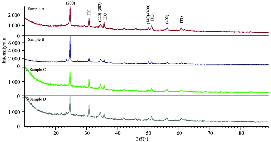 | Fig.1 XRD patterns of the WO3 thin films deposited by CSP and SC techniques |
2 Results and Discussion
Panalytical Empyrean model X-ray diffractometer was used for XRD spectra (λ =1.540 6 Å ). In Figure 1, XRD spectra of the films are seen. WO3 thin films have more intense peaks compared to ITO peaks. The most intense peak at (200) plane was observed for all of the thin films in the XRD spectra. Among them, the WO3 thin film deposited by CSP technique using 100 mL precursor solution (sample B) has more intense peak at (200) than others. Otherwise, the WO3 thin film deposited by CSP technique using 50 mL precursor solution can be sharp (200) peak when the sample was annealed at 500 ℃. Additionally, the film deposited by SC technique and annealed at 500 ℃ (Sample D) has more intense (200) peak than the film deposited by SC technique and annealed at 400 ℃ (sample C). In the literature, it is explained that the room temperature crystallographic structure of WO3 is derived from the ReO3 structure with the corner shared octahedral tilted, the tungsten atoms distorted from their symmetrically located positions within the oxygen octahedra, to form zig-zag chains with alternating short and long W-O bond distances and WO3 is possible to have different polymorphs such as monoclinic (> 17~330 ℃), orthorhombic (330~740 ℃) and tetragonal (> 740 ℃) at the devices operation conditions[15]. According to XRD patterns, crystal structure of the WO3 thin films probably belongs to monoclinic crystal phase (PDF#43-1035), however triclinic (PDF#20-1323) and orthorhombic (PDF#20-1324) WO3 crystal systems have approximately same d values at (200) plane. Detail of XRD results is given in Table 1.
| Table 1 d values, 2 theta values and (h k l) indices ( Sample A-B-C-D) |
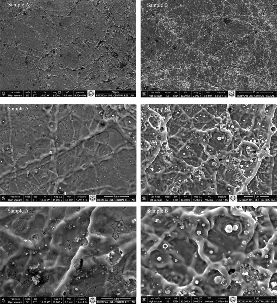 | Fig.2 SEM images of the WO3 thin films deposited by CSP technique [Sample A and Sample B] |
FEI Quanta 550 FESEM model Scanning Electron Microscopy was used for surface morphology of the samples. In Fig.2 and Fig.3, it is seen SEM images at the magnification of 2 000, 15 000 and 30 000 for all of the samples.
As seen in Fig.2, micro fibrous reticulated (network like) morphology is observed for the Sample A and Sample B and it is known that metal oxide structures shows usually fiber reticulated (chain) morphology at different dimensions throughout the surface[16, 17].
SEM images of the WO3 thin films synthesized with SC technique are seen in the Fig.3. In both samples, it is observed smooth and homogenous morphology throughout the surface. Additionally, it is seen that Tungsten oxide clusters are more intense on surface for the Sample D.
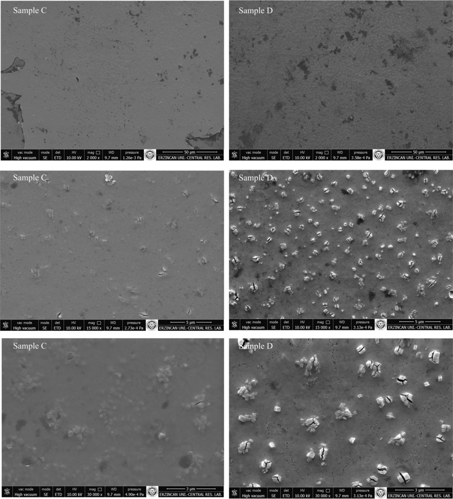 | Fig.3 SEM images of the WO3 thin films deposited by SC technique [Sample C and Sample D] |
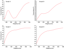
PerkinElmer Model Spectroscopy was used for UV-Vis spectra of the samples. As seen in Fig.4, when the solution amount increases, a transmittance decreases because of the increasing thickness of the film. In Fig.4, it is observed that sample A shows maximum (approximately 92%) transmittance and Sample B shows minimum transmittance (approximately 50%) among all of the samples. However, sample C and D show approximately 80% transmittance. These results are consistent with the literature[18, 19].
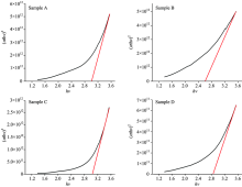
Absorption coefficient can be calculated by using optical transmittance spectra. Absorption coefficient (α ) is given with the following equation for semiconductor materials;
Eg is the optical band gap, hν is the photon energy and n is the constant equal to 1/2 for direct transition and 2 for indirect transition[17] and t is thickness of the films.
In Figure 5, It is seen that (hν )-(α hν t)2 graphs which is used for calculating optical band gap of WO3 thin films.
It is observed that optical band gap of the samples changes at the range of 2.6 to 3.1 eV. These values are consistent with the literature[20].
Gamry Model Potentiostat was used for Cyclic Voltamograms of the samples. The prepared solution!for intercalation (adding ion) and deintercalation (extraction of ion) processes was obtained by dissolving of LiClO4 in PC electrolyte solution (molarity of 0.3 and 30 mL).
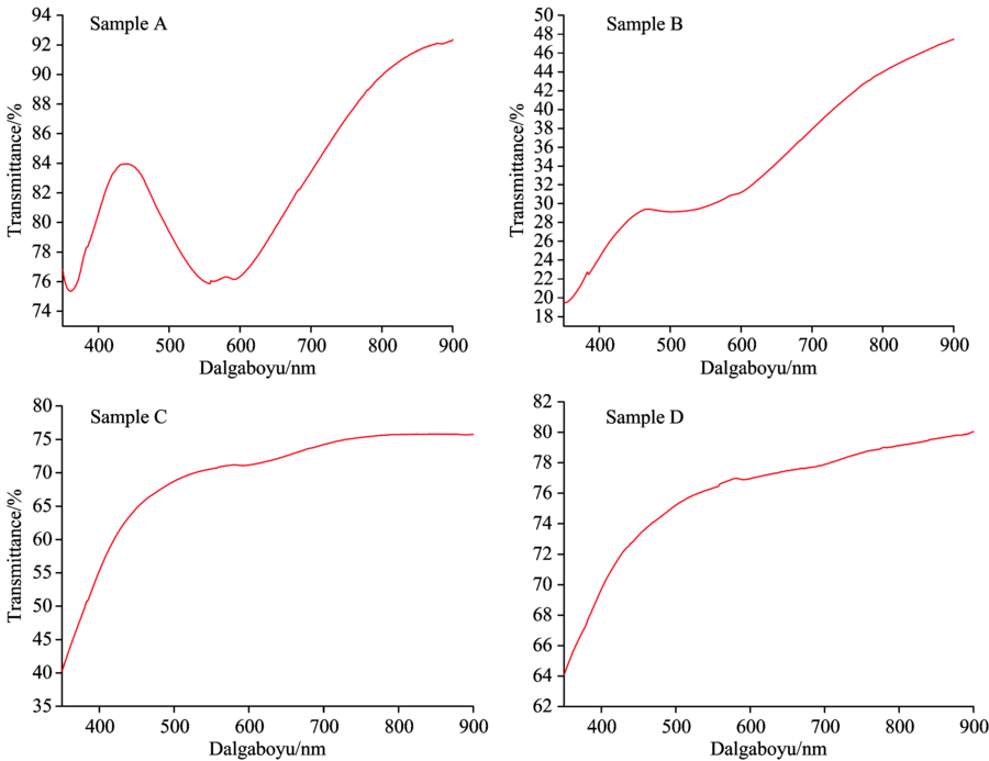 | Fig.4 UV-Vis spectra of the WO3 thin films deposited by CSP and SC techniques (Transmittance (%)-Wavelength (nm)) |
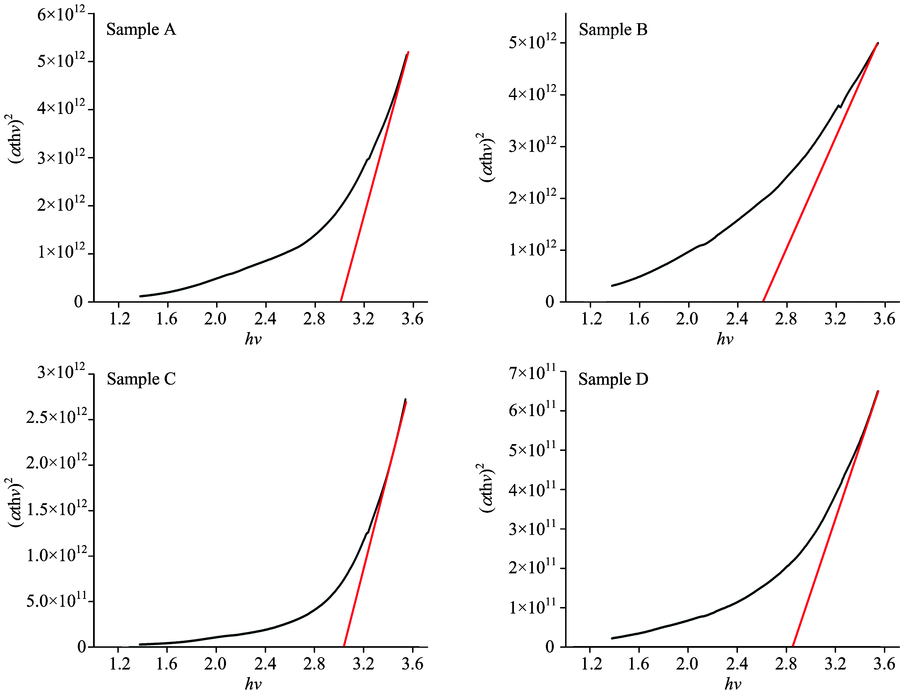 | Fig.5 Eg(hν )-(α hν t)2 spectra of the WO3 thin films deposited by CSP and SC techniques |
The CV measurements were obtained between -1.5 V to 500 mV and -500 mV to 500 mV with scanning rates of 500 mV· s-1. During the electrochemical process, the following reaction occurs:
WO3 thin film turns to blue color during intercalation ions to WO3 lattice and it turns to transparent during de-intercalation ions from the lattice.
In Fig.6, it is seen that CV measurements of the thin films were obtained with CSP and SC Technique. It is clear that Sample B shows better electrochromic performance due to maximum curve area between anodic scanning and cathodic scanning. If the anodic scanning is tangent to cathodic scanning, material does not show any electrochromic feature. According to CV analysis, anodic peak emerged sharper in the sample B.
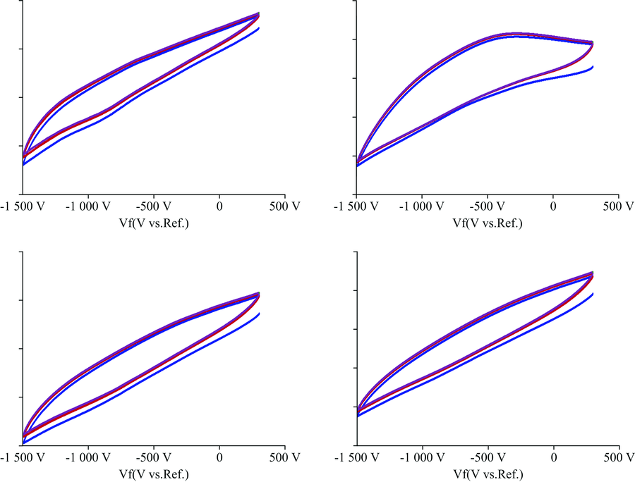 | Fig.6 Cycling Voltammograms of the WO3 thin films deposited by CSP and SC Techniques |
3 Conclusions
As a result, in this study Tungsten Trioxide thin films were synthesized by using two simple solution-based economical techniques. According to XRD patterns of the WO3 thin films, the film thickness and WO3 peak intensity of (200) plane increase depending on the increase of the solution amount. In addition to this, percentage of transmittance decreases depending on the increase of film thickness. According to SEM images of the films deposited by CSP technique, more distinctive and more fibrous reticulated layers were observed depending on the increase of amount of solution. It is seen that WO3 thin films deposited by the CSP technique can be used in electrochromic applications. According to XRD patterns of the WO3 thin films deposited by SC technique, the (200) peak intensity increases depending on increasing annealed temperature. According to UV-Vis spectra, more transparent films are obtained depending on high annealing temperature for the thin films deposited by SC. Particle size and surface homogeneity of the films prepared with this method are quite well. A disadvantage of the SC technique is the long duration of the coating process. Although the films obtained with both techniques can be used in electrochromic applications, it is obvious that the thin films deposited by CSP technique using 100 ml solution shows better electrochromic performance.
The authors have declared that no competing interests exist.
参考文献
| [1] |
|
| [2] |
|
| [3] |
|
| [4] |
|
| [5] |
|
| [6] |
|
| [7] |
|
| [8] |
|
| [9] |
|
| [10] |
|
| [11] |
|
| [12] |
|
| [13] |
|
| [14] |
|
| [15] |
|
| [16] |
|
| [17] |
|
| [18] |
|
| [19] |
|
| [20] |
|