


非对称银纳米双环表面等离激元光谱特性
[史冬冬1  , 张悦
, 张悦1 , 孙诚1, 2, * ]
, 张悦]
|
|


作者简介: 史冬冬, 1996年生, 大连大学物理科学与技术学院硕士研究生 e-mail: 805194352@qq.com
贵金属纳米材料在入射光激发下能够产生表面等离激元, 即金属表面自由电子产生集体振荡。 当其振荡频率与入射光频率相同时, 发生表面等离激元共振, 形成一种特殊的电磁场模式和光谱特性。 利用该电磁场模式和光谱特性, 能够调节金属纳米材料的光谱学行为, 例如通过改变金属纳米结构的大小、 形状以及周围介质介电常数等参数, 在微纳尺度上实现光谱学信号的有效调控。 目前, 除了具有一定对称性的贵金属纳米材料被大量研究和应用外, 非对称纳米结构的表面等离激元光谱特性也受到广泛关注。 研究表明, 在可见-近红外波段光谱范围内设计表面等离激元光电传感器件的关键问题在于, 如何有效地调节其消光谱的共振波长、 半峰宽以及峰值强度等主要特征参数。 提出一种基于银纳米双环组成的非对称结构, 利用时域有限差分方法, 在可见-近红外波段内, 通过分别改变银纳米双环的尺寸、 间距及入射光偏振方向等参数, 计算了该纳米结构在不同条件下的消光谱。 结果表明, 在0.4~3 μm的消光谱内, 入射光能够激发产生两个独立的表面等离激元共振峰。 通过研究峰值波长处的电场分布图发现, 上述共振峰分别对应两种不同的电磁场模式。 结果还表明, 消光谱内两个独立的共振峰可以通过改变该双环结构的不同参数, 被分别地进行调节。 其中, 可以通过改变该双环结构的半径来有效调节短波长峰的共振波长和半峰宽, 同时保持长波长峰的共振波长和半峰宽基本不变。 此外, 通过改变两环间距或入射光偏振方向, 可以分别以不同趋势来调节两个共振峰的峰值强度。 在提出的非对称银纳米双环的消光谱中, 获得了能够被分别调节的两个表面等离激元共振峰, 研究结果能够为可见-近红外波段内基于银纳米材料光电传感器件的开发设计提供理论基础。
The incident light may induce surface plasmons noble-metal nanomaterials, which are the collective oscillations of the surface electrons in the metal. When the frequency of the surface plasmons matches the incident light, plasmonic resonance occurs with a special electro-magnetic and spectral property. Ultilizing this property, the spectral behavior of metallic nanomaterials can be adjusted. For example, by varying paramters including the size, shape, and dielectric constants the nanostructures’ background materials, the spectral signals can be effectively controled. So far, the surface plasmons of noble-metal nanomaterials with certain symmetries have been widely studied and applied. In addition, the spectral properties of asymmetric metallic nanostructures have also drawn great attention in the community. It has been shown that one important problem in designing plasmonic optical sensors in the visile-near infrared regime is how to achieve the effective control of key parameters of the extinction spectra, including the resonance wavelength, spectral width, and peak intensity. In this work, an asymmetric structure consisting of two silver nanorings is proposed. With the finite-difference time-domain method, the nanostructure’s extinction spectra are studied in the visible-near infrared regime by varying the parameters, including the rings’ radii, the separation, and the light’s polarization. The results indicate that two independent surface plasmons resonances are induced in the extinction spectra in the wavelength range of 0.4~3 μm. It is found from the electric fields that the resonances are correlated to two different electro-magnetic modes. It is also revealed that the two different resonance peaks in the extinction spectra can be independently adjusted by changing different parameters of the double nanorings. The shorter resonance wavelength and its spectral width can be tuned by varying the sizes of the nanorings, while the longer resonance wavelength and its spectral width can remain almost the same. Besides, The peak intensities of the two resonances can be adjusted in different trends by changing the nanorings’ separation or the polarization angle of the incident light. In this work, two plasmonic resonance peaks that can be respectively controled are revealed in the extinction spectra of the asymmetric silver double nanorings; the results shown in this work may provide us with theoretical foundations in the design of photoelectric sensors in the visible-near infrared region.
在入射光激发下, 金属表面自由电子会产生集体振荡, 和相应的电磁场一起, 能够形成具有特定能量和频率的表面等离激元(surface plasmons, SPs)。 当入射光与表面等离激元的频率相同时, 两者被有效耦合, 能量和动量发生高效转移, 形成一种特殊的电磁场模式, 被称为表面等离激元共振(surface plasmons resonance, SPR)。 随着微纳工艺和仿真计算的发展, 表面等离激元已被广泛应用于传感器件、 表面拉曼增强、 亚波长光学、 光子器件和生物医学等领域[1, 2, 3]。
目前, 人们发现具有一定对称性的贵金属纳米材料能够展现出良好的表面等离激元和相关的光谱特性。 例如, 通过对一个银纳米圆环的系统计算发现, 偶极、 四极和八极表面等离激元共振模式均能够产生, 对称的电场分布以及在可见-近红外波段内的局域电场增强也均可实现[4]。 在对银纳米圆柱阵列的近场光学特性研究中发现, 可以通过调节圆柱的间距来获得高的局域电场增强[5]。 利用离散偶极近似方法, 可以获得同心铝环/盘纳米孔洞结构的消光谱和电场分布, 其结果表明该纳米结构不仅具有强局域电场, 而且在可见光波段还展现出可调节的正键键合共振模式[6]。 此外, 在对同心银环/盘结构的研究中, 表面等离激元耦合和吸收增强也有报道[7]。 通过对一种基于双扇面银纳米结构的仿真计算发现, 多种表面等离激元共振模式被激发, 其在低能带区域相对应的电场增强被显著提高[8]。 最近, 利用有限元方法对金属纳米球-纳米圆盘结构进行的研究表明, 在径向偏振光激发下, 能够形成纵向电场有效增强的间隙模式等离激元共振, 其可被用于表面增强拉曼测量[9]。
近年来, 除了针对具有对称性贵金属纳米结构的表面等离激元研究之外, 由于对称性的破缺可能带来更为丰富多变的光谱特性, 进而为光电传感器件的设计提供更多选择, 因而对非对称纳米结构表面等离激元光谱性质的研究也同样备受关注[10, 11]。 例如, 利用有限元方法, 在对由两个大小不同的环/盘孔洞组成的纳米结构表面等离激元的研究中发现, 该结构能产生多极模式且能够被独立调节[12]。 本研究提出了一种非对称银纳米双环结构, 利用时域有限差分方法, 在可见-近红外波段范围内, 通过改变结构参数, 系统研究其表面等离激元光谱性质。
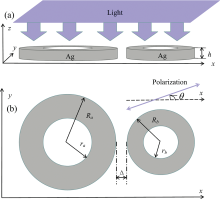
提出的非对称银纳米双环结构如图1所示。 图1中, 在x-y平面内放置厚度均为h的两个银环。 两圆环大小不同, 内外半径分别用ra, Ra, rb和Rb表示。 两环圆心的y轴和z轴坐标相同。 如图1(a)所示, 平面波入射光沿z轴负方向垂直入射。 如图1(b)中所示, 线偏振入射光的电场矢量与x轴之间的夹角为θ , 即当θ =0° 时, 入射光沿x偏振; 当θ =90° 时, 入射光沿y偏振。
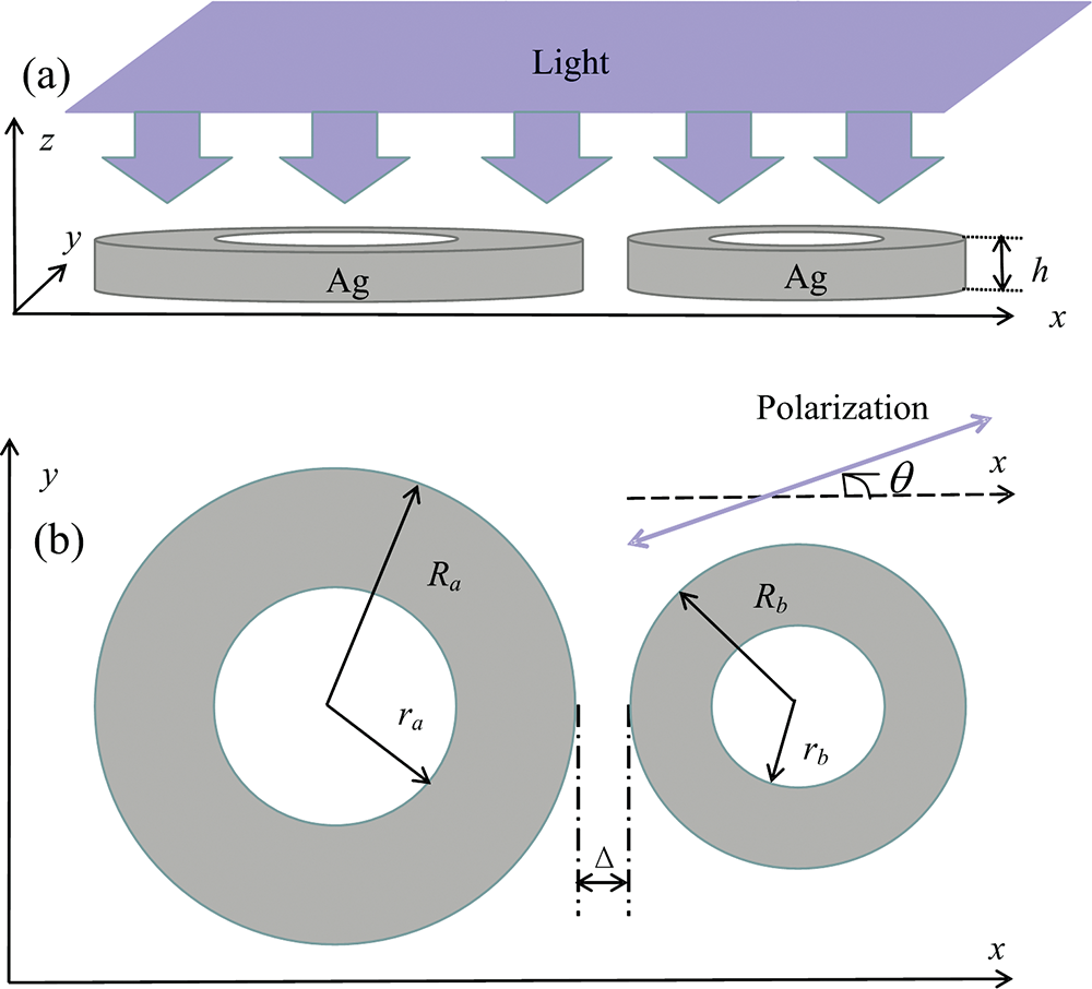 | 图1 非对称银纳米双环结构图 (a): 侧视图; (b):俯视图 图中h为圆环厚度, Δ 为两环间距, ra, Ra, rb和Rb分别为两圆环内外半径; 平面波入射光沿z轴负方向垂直入射; 线偏振入射光的偏振角(θ )定义为在x-y平面内其电场矢量与x轴之间的夹角Fig.1 Schematic structure of the asymmetric silver double nanorings (a): Cross section; (b): Top view h is the thickness of the rings, Δ is the separation between the rings, and ra, Ra, rb, and Rb are the inner and outer radii of the rings, respectively; A plane-wave light is normally incident along the -z axis; The polarization of the polarized light, θ , is defined as the angle between the electric vector and the x axis in the x-y plane |
本研究利用时域有限差分方法(FDTD)计算完成。 时域有限差分方法是对麦克斯韦方程组的一种差分表示, 在电场和磁场节点空间和时间上采用交错抽样, 用来解决电磁波在介质中传播等相关问题。 计算中x, y和z方向上均使用完全匹配层(PML)边界条件, 入射光的波长范围为0.4~3 μ m。 所有计算中的网格选取均小于最短波长的1/10, 以避免由该仿真方法所引起的误差。 本研究中银的介电常数由文献[13]中的实验数据给出。
通过对图1所示结构的仿真模拟, 计算出该双环结构在不同波长下的散射截面和吸收截面, 进而获得其消光效率(Qext)[14]。 当计算出消光效率在全波长范围内随波长变化的曲线后, 即获得了该纳米结构的消光谱。
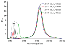
随着两个纳米环相对尺寸的改变, 该结构的非对称性程度也会发生变化, 进而影响其表面等离激元特性。 首先固定大圆环半径, 逐步改变小圆环半径, 计算此双环结构的消光谱, 结果如图2所示。 大圆环固定为Ra=100 nm, ra=80 nm, 两环中心点之间的距离也固定为320 nm。 小圆环的外半径从30 nm增加到50 nm, 内半径相应地从10 nm增大到30 nm。 观察图2可知, 对于任何一条消光谱曲线, 均在不同波长处出现两个明显的峰, 分别用α 和β 标记。 消光谱的双峰特征表明, 该双环结构能够在入射光的激发下, 在500~900和1 600 nm两个波段附近分别产生表面等离激元共振现象。 为进一步明确上述两个波段处共振行为的物理图像, 对α 峰和β 峰波长下的电场分布进行了计算, 结果由图3给出。
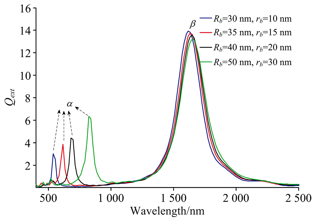 | 图2 不同小圆环半径下的消光谱 大圆环的尺寸固定, 半径均为Ra=100 nm, ra=80 nm; 两圆环高度均为h=10 nm; 两环中心点之间的距离固定, 均为Ra+Rb+Δ =320 nm; 入射光均为x偏振光Fig.2 Extinction spectrum as a function of the radii of the smaller nanoring The radii of the larger ring were fixed to be Ra=100 nm, ra=80 nm; The thicknesses of the rings were both h=10 nm; The distance between the rings’ centers was fixed to be Ra+Rb+Δ =320 nm; The light was x-polarized |
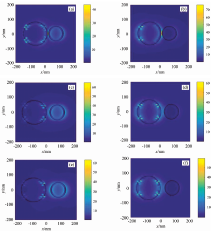
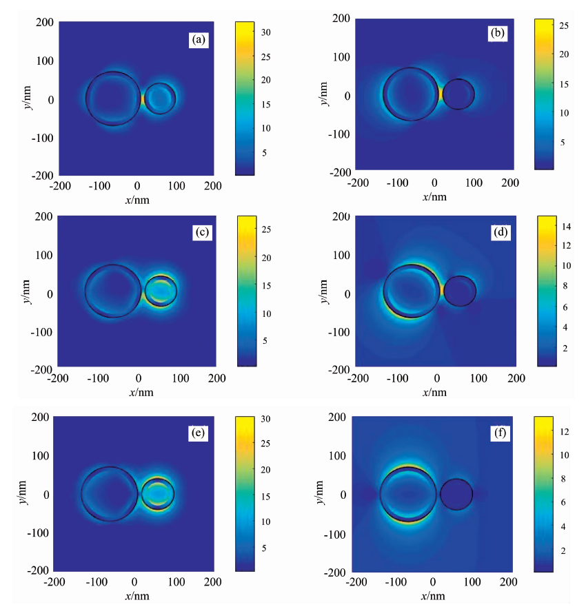
 | 图3 对应于图2中峰值波长下, x-y平面内的电场分布图 图中, (a)和(b)分别对应Rb=30 nm时的α 峰和β 峰; (c)和(d) Rb=40 nm时α 峰和β 峰; (e)和(f) Rb=50 nm时α 峰和β 峰; 为简洁起见, 只有两个环的外侧边缘位置在图中用圆圈实线标记出来, 以方便观看Fig.3 Distributions of the electric fields in the x-y plane, corresponding to the peaks of the extinction spectra shown in Fig.2 In the figure, (a) and (b) represent Peak α and Peak β for Rb=30 nm, respectively; (c) and (d) Peak α and Peak β for Rb=40 nm, respectively; (e) and (f) Peak α and Peak β for Rb=50 nm, respectively; To guide the eye, the positions of the rings are indicated in solid circles in the figures |
图3中, 将Rb=30, 40和50 nm对应的电场分布作为实例给出。 图3(a), (c)和(e)对应于α 峰的电场, 而β 峰的电场由图3(b), (d)和(f)中给出。 比较图3中左右两侧结果可知, α 峰和β 峰对应两种不同的电场分布。 说明图2消光谱中, 两个峰值波长处对应的表面等离激元共振具有不同的电磁场模式。 其中, α 峰对应的电场主要分布在小圆环表面, 而β 峰则主要集中在大圆环表面。 这与α 峰出现在较短波长处(500~900 nm), 以及β 峰出现在较长波长处(1 600 nm)这一现象相符合。 值得一提的是, 仔细观察图中左右两侧α 峰和β 峰分别对应的电场可以发现, β 峰处电场分布[如图3(b)]中小圆环表面电场很弱, 而α 峰[如图3(a)]中大圆环表面电场不是很弱, 仍然可被观测到, 这可能与两圆环间的耦合作用相关。
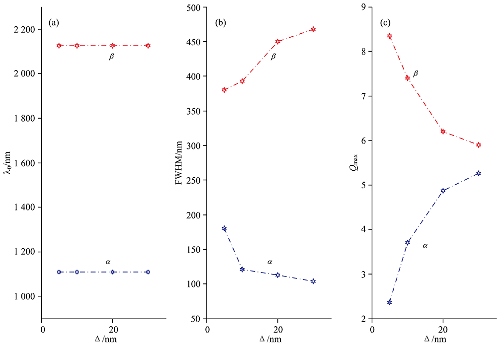
为了定量分析图2中消光谱的两个共振峰特性, 将α 峰和β 峰分别对应的共振波长(λ 0)、 半峰宽(FWHM)和峰值强度(Qmax)等三个特征参数的数值从图2中提取出来, 结果在图4中给出。
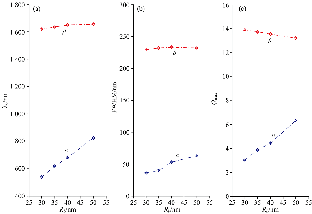 | 图4 对应于图2消光谱中α 峰和β 峰的(a)共振波长(λ 0), (b)半峰宽(FWHM)和(c)峰值强度(Qmax)Fig.4 (a) The resonance wavelengths (λ 0), (b) the full width at half maximum intensities (FWHM), and (c) the peak intensities (Qmax) for Peak α and Peak β of the extinction spectra shown in Fig.2 |
观察图4(a, b, c)可知, 对于波长较长处的β 峰而言, 在小圆环尺寸逐渐增加的情况下, 共振波长、 半峰宽以及峰值强度, 都没有明显的变化; 与图2中定性的观察结果相一致。 然而, 对于波长较短处的α 峰, 随着小圆环半径逐渐增加, 上述三个特征参数均出现了明显的增大趋势。 共振波长从538 nm增长到824 nm, 半峰宽从36 nm增加到63 nm, 峰值强度也从3.0增加到6.3。 图4给出的定量结果及规律, 能够给传感器件设计提供一个较好的平台, 如利用β 峰对于圆环尺寸不敏感的特点, 给系统定标, 而变化明显且规律性强的α 峰可以用于传感相关的测量。
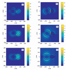
除了圆环尺寸之外, 两环之间的间距也是该结构的一个可调参数, 对其产生的相应规律也进行了仿真计算。 图5给出了不同间距(Δ )下, 非对称双环结构的消光谱。 图5中, 间距从5 nm到30 nm逐渐增加, 同时, 两圆环的尺寸均保持不变。 从图5结果可知, 对于任意一个间距条件下, 消光谱曲线均出现α 和β 两组峰, 对应于两个波段处的表面等离激元共振。 类似于对半径的研究, 相应于图5中α 和β 两组峰的电场分布也分别计算出来, 不同间距下的电场结果在图6中给出。 类似于图3, 通过比较图6中(a, c, e)与(b, d, f)分别代表的α 峰和β 峰电场分布的不同, 可以获得和图3相似的规律, 即消光谱曲线上的两组共振峰分别归属于入射光在不同波段处的两种电磁场模式。
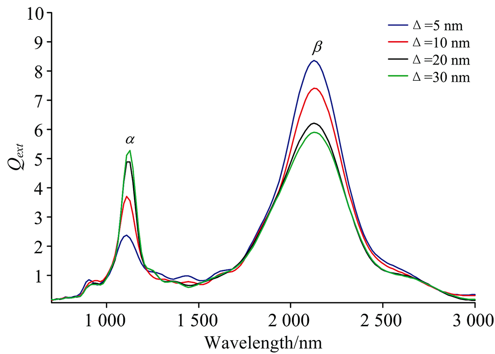 | 图5 不同间距下的消光谱 两圆环的半径均固定, 分别为Ra=80 nm, ra=70 nm, Rb=50 nm, rb=40 nm; 两圆环高度均为h=10 nm; 入射光均为x偏振光Fig.5 Extinction spectrum as a function of the separation between the nanorings The radii of the rings were fixed to be Ra=80 nm, ra=70 nm, Rb=50 nm, and rb=40 nm, respectively; The thicknesses of the rings were both h=10 nm; The light was x-polarized |
 | 图6 对应于图5中峰值波长下, x-y平面内的电场分布图 其中, (a)和(b)分别对应Δ =5 nm时的α 峰和β 峰; (c)和(d)Δ =20 nm时α 峰和β 峰; (e)和(f)Δ =30 nm时α 峰和β 峰Fig.6 Distributions of the electric fields in the x-y plane, corresponding to the peaks of the extinction spectra shown in Fig.5 In the figure, (a) and (b) represent Peak α and Peak β for Δ =5 nm, respectively; (c) and (d) Peak α and Peak β for Δ =20 nm, respectively; (e) and (f) Peak α and Peak β for Δ =30 nm, respectively |
从图5消光谱曲线中提取出α 峰和β 峰特征参数的具体数值, 在图7中给出。 观察图7(a)和(b)可知, 随着两环间距的增加, α 峰和β 峰的共振波长, 几乎没有发生变化, 而α 峰的半峰宽逐渐减小, β 峰的半峰宽逐渐增大; 这一点与图4中给出圆环半径的影响有明显不同。 此外, 从图7(c)可以看到, 随着间距的增加, 两峰的强度产生了不同的变化规律。 α 峰逐渐变强, 而β 峰逐渐减弱。 结合α 峰和β 峰的共振波长对间距不敏感这一现象, 本文提出的非对称双环结构中Δ 这一参数, 可以被进一步利用到前面提到的传感器件设计中。 如用β 峰进行定标时, 可以适当减小Δ 的数值, 以增加峰值强度; 而用α 峰进行传感测量时, 可以通过增加间距来提高信号强度。
 | 图7 对应于图5消光谱中α 峰和β 峰的(a)共振波长(λ 0), (b)半峰宽(FWHM)和(c)峰值强度(Qmax)Fig.7 (a) The resonance wavelengths (λ 0), (b) the full width at half maximum intensities (FWHM), and (c) the peak intensities (Qmax) for Peak α and Peak β of the extinction spectra shown in Fig.5 |
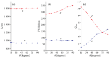
除了半径和间距, 还研究了入射光偏振角对该双环结构的影响, 相应的消光谱由图8给出。 在不同的偏振角情况下, 图8给出的消光谱也都表现出了两个共振峰的特性。 因此, 相应于α 峰和β 峰, 电场分布图也进一步由计算得到, 在图9中给出。 观察图9可知, 尽管α 峰和β 峰对应的电场取向在x-y平面内均随着偏振角的增加, 从沿x轴方向[如图9(a)和(b)]逐渐转到沿y轴方向[如图9(e)和(f)], 但是通过比较左右两侧的电场可知, 对于任意一个偏振角度而言, α 峰和β 峰所表现的共振仍然在两个波段处具有不同的电磁场模式。 最后, 从图8消光谱中提取出的共振峰特征参数, 在图10中给出, 由此对α 峰和β 峰在偏振角变化时的规律进行定量分析。
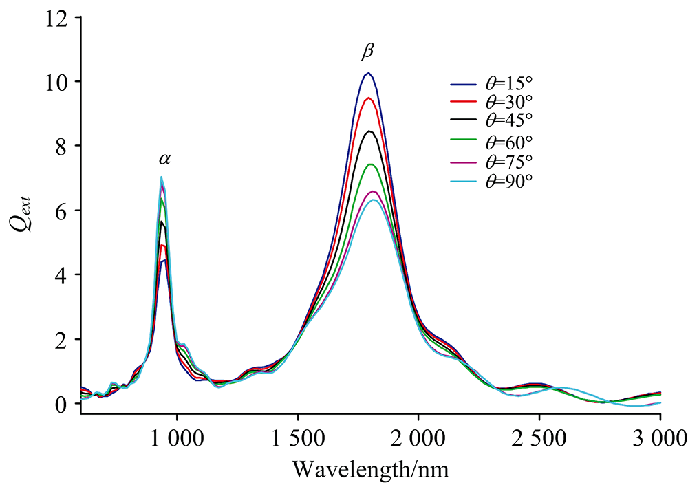 | 图8 不同偏振角时的消光谱 两圆环的半径均固定, 分别为Ra=70 nm, ra=60 nm, Rb=40 nm, rb=30 nm; 两圆环高度均为h=10 nm; 两圆环之间的间距固定为Δ =10 nm; 入射光偏振角(θ )的定义如图1(b)所示Fig.8 Extinction spectrum as a function of the polarization angle of the incident light The radii of the rings were fixed to be Ra=70 nm, ra=60 nm, Rb=40 nm, and rb=30 nm, respectively; The thicknesses of the rings were both h=10 nm; The separation between the rings was fixed to be Δ =10 nm; The polarization angle of the light (θ ) was indicated in Fig.1(b) |
 | 图9 对应于图8中峰值波长下, x-y平面内的电场分布图 其中, (a)和(b)分别对应θ =15° 时的α 峰和β 峰; (c)和(d)θ =60° 时α 峰和β 峰; (e)和(f)θ =90° 时α 峰和β 峰Fig.9 Distributions of the electric fields in the x-y plane, corresponding to the peaks of the extinction spectra shown in Fig.8 In the figure, (a) and (b) represent Peak α and Peak β for θ =15° , respectively; (c) and (d) Peak α and Peak β for θ =60° , respectively; (e) and (f) Peak α and Peak β for θ =90° , respectively |
图10(a)的结果表明, 随着入射光偏振角的增加, α 峰和β 峰的共振波长未发生明显的变化, 说明其对入射光电场矢量在x-y平面内的取向变化不敏感。 这一规律可以进一步应用到前面提到传感器件的设计中, 即本文提出非对称纳米双环结构的两个共振峰波长参数, 对于入射光的偏振性具有一定的容忍度。 从图10(b)中可知, α 峰的半峰宽随偏振角变化不大, 而β 峰的半峰宽则随偏振角增大而增加。 此外, 图10(c)给出的峰值强度随偏振角的变化规律, 相对于α 峰和β 峰具有不同的变化趋势; 类似于对图7(c)的讨论, 这一特性也可以被合理利用, 以分别调节α 峰和β 峰所对应的信号强度。
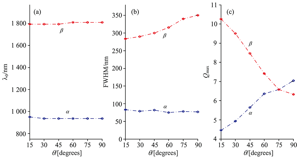 | 图10 对应于图8消光谱中α 峰和β 峰的(a)共振波长(λ 0), (b)半峰宽(FWHM)和(c)峰值强度(Qmax)Fig.10 (a) The resonance wavelengths (λ 0), (b) the full width at half maximum intensities (FWHM), and (c) the peak intensities (Qmax) for Peak α and Peak β of the extinction spectra shown in Fig.8 |
提出了一种非对称银纳米双环结构, 利用时域有限差分方法, 在可见-近红外波段范围内, 通过分别改变圆环半径、 两环间距以及入射光偏振角等参数, 研究了该纳米结构的消光谱和峰值电场等表面等离激元特性。 结果表明, 在不同波段内, 入射光能够分别激发产生表面等离激元共振, 且分别对应两种不同的电磁场模式。 此外, 定量分析发现, 共振峰所对应的共振波长、 半峰宽和峰值强度均可被分别调节。 其中, 改变圆环半径可以作为一种有效手段, 通过利用两个共振峰的不同变化规律来进行传感器件的开发设计。 本工作的主要结论对于可见-近红外波段内, 基于贵金属纳米材料表面等离激元的光电器件设计具有理论价值。
| [1] |
|
| [2] |
|
| [3] |
|
| [4] |
|
| [5] |
|
| [6] |
|
| [7] |
|
| [8] |
|
| [9] |
|
| [10] |
|
| [11] |
|
| [12] |
|
| [13] |
|
| [14] |
|