
电镀法在氧化铟锡上制备铜锌锡硫薄膜的光谱特征
[宋思悦 , 刘旭炜, 林鸿霄, 王学进
* , 何志巍]
, 刘旭炜, 林鸿霄, 王学进, 何志巍]
|
|


低成本、 环境友好的铜锌锡硫替代含贵金属和有毒金属的铜铟镓硒, 是薄膜太阳能电池的最佳选择。 电镀法是一种无需真空设备和靶材的低成本方法。 一种更简单的制膜方法是在水溶液中共电镀沉积Cu-Zn-Sn(CZT)合金于FTO衬底上。 采用氩气保护气氛下在550 ℃硫化电镀法制得的CZT合金前驱体, 成功制备了CZTS薄膜。 采用三电极体系将CZT合金前驱体电镀在FTO上, 其中FTO作为工作电极, 铂(Pt)网和Ag/AgCl分别作为对电极和参比电极。 电解质由CuSO4, ZnSO4, SnSO4, 络合剂-三乙醇胺(TEA)和柠檬酸钠组成。 前驱体在氩气保护气氛下550℃硫化得到CZTS薄膜。 采用X射线衍射(XRD)、 拉曼光谱、 扫描电子显微镜(SEM)、 紫外可见光光谱仪和光电化学测量(PEC)等方法, 表征了CZTS薄膜的结构、 形貌、 成分和光谱学性质。 XRD和拉曼光谱证明了550 ℃硫化后的CZTS薄膜具有锌黄锡矿结构。 一个Raman主峰位于342 cm-1, 两个Raman次强峰分别位于289和370 cm-1, 这些峰位与锌黄锡矿CZTS的峰位相吻合。 SEM结果证明优化后CZTS薄膜成分接近CZTS的理想化学计量比, CZTS薄膜中Cu/(Zn+Sn)和 S/(Zn+Sn+Cu)分别为0.52和1.01, 这表明CZTS薄膜中S的含量非常合适。 PEC结果证实, 采用前照射或后照射FTO/CZTS均产生光电流, 并且两种照射下产生的光电流方向一致。 通过紫外可见光光谱测量并由此计算出的CZTS能隙为1.45 eV。 通过上述分析证明制备的CZTS薄膜具有高品质, 可用于制备CZTS薄膜太阳能电池。
SONG Si-yue, (1994—), master, College of Science, China Agricultural University e-mail: yue2605@163.com
Low cost and environment friendly Cu2ZnSnS4 (CZTS) is the best candidate to replace CuIn xGa1- xSe2 (CIGS) which owns noble and toxic metal for thin film solar cells. Electrodeposition technique is a low cost method where vacuum equipment and target materials are not required. A simpler fabrication method is co-electrodeposition of Cu-Zn-Sn (CZT) alloy on fluorine-doped tin oxide (FTO) in aqueous solution. In this paper, CZTS thin films were successfully prepared by sulfurization of electrodeposited CZT alloy precursors at 550oC in protective argon gas. The CZT precursors were electrodeposited on FTO via a three-electrode system in which FTO is used as working electrode, platinum (Pt) mesh and Ag/AgCl as counter and reference electrodes. The electrolyte contains CuSO4, ZnSO4, SnSO4, complexing agent-Triethanolamine (TEA) and sodium citrate. The precursors were sulfurized by sulfur vapor at 550 ℃ in protective argon gas and then CZTS films were obtained. The structural, morphological, compositionaland optical properties of CZTS films have been characterized by X-ray diffraction (XRD), Raman spectroscopy, scanning electron microscopy (SEM), UV-vis spectroscopy and photoelectrochemical measurement (PEC). XRD and Raman spectroscopy have confirmed the kesterite structure of CZTS films sulfurized at 550 ℃. One major peak at 342 cm-1 and two second strong peaks at 289 and 370 cm-1 are observed in the Raman spectra, which agree with those reported from kesterite CZTS. SEM shows chemical composition of optimum CZTS film is near that of stoichiometric CZTS. The ratios of Cu/(Zn+Sn) and S/(Zn+Sn+Cu) in CZTS film are 0.52 and 1.01, respectively, which indicates that the content of S in “copper poor” CZTS film is very suitable. The photocurrent of the “copper-poor” CZTS film was measured by PEC. PEC results confirm that light current is produced by FTO/CZTS under front/back irradiation, and the photocurrent flows in the same direction in both cases. The band gap of CZTS is 1.45 eV. It is shown that high-quality CZTS thin films have been prepared via above analysis.
In the past few decades, solar energy as a sustainable and clean energy has become a new impetus to many countries in seeking economic development. The thin film solar cells based on polycrystalline CdTe and CuIn(Ga)Se2 (CIGS) absorption layers have been developed very fast, and they have already been commercialized with stable power conversion efficiencies of over 20 percent[1, 2]. But toxic metal such as Cd and noble metals like In, Ga, Te directly limit their commercialization. Therefore, searching for a low cost, environmental harmless, non-toxic and abundant elements has become a very hot research topic. The Cu2ZnSnS4 (CZTS) that is composed of abundant materials without using any rare metals is the best candidate to replace CIGS[3, 4, 5, 6]. CZTS is also an interesting material as an absorber layer in a thin film solar cell because of a large absorption coefficient over 104 cm-1 and of a suitable band-gap energy of 1.4~1.5 eV[5, 7, 8]. For these reasons, CZTS is one of the most promising new green photovoltaic materials for thin film solar cells and it is very suitable for low cost large-scale commercial production. Katagiri et al.[4] fabricated the first CZTS film semiconductor by electron-beam evaporation and its conversion efficiency was 0.66%. However, single-phase CZTS has many problems such as small existence range, difficult quaternary synthesis, and so on. It is still under investigation. In recent years, with the rapid development of science and technology, the research of CZTS film has gradually matured. IBM[9] company used thermal evaporation method to prepare the devices with efficiency of 8.4%. The National Renewable Energy Laboratory (NREL)[10] of United States prepared the 9.15% efficiency for devices by thermal evaporation. Later, IBM[11] prepared device with 9.66% efficiency by hydrazine solution, The device efficiency had reached to 12.6% through continuous optimization[12]. At present, the conversion efficiencies of thin film solar cells based on CZTS prepared by vacuum method (NREL) and non-vacuum method (IBM) have reached their world records respectively. Although these methods can acquire higher efficiency, they cannot allow large area product in industry. Electrodeposition technique is superior to the above methods where vacuum equipment and target materials are not required[13, 14, 15]. IBM[16] reports that they have fabricated a champion CZTSSe solar cell among electrochemical deposition with 7.0% efficiency via sequentially electrodepositing copper, tin and zinc in organic liquor. A simpler fabrication method is co-deposition of Cu-Zn-Sn (CZT) alloy on fluorine-doped tin oxide (FTO) in aqueous solution. Co-deposition is one of the best methods due to its simplicity and capability for large area deposition, as well as its low costs[17, 18, 19, 20, 21, 22]. In this paper, we add a new reagent-Triethanolamine (TEA) into the electrolyte. It works with sodium citrate to make CZT precursors smoother and denser. Furthermore, device should absorb light as much as possible. Bifacial illumination and absorption is a promising way to meet the requirements. Therefore, we use transparent conducting glass (FTO) which can be made into bifacial solar cells. The bifacial solar cells present high photoelectrical conversion efficiency and can reduce the cost of solar electricity relative to monofacial solar cells[23, 24]. These devices will also be prone to electron-hole pair generation upon illumination in both sides simultaneously[25]. This paper focuses on these simpler fabrication methods and bifacial absorption process.
In this experiment we cut FTO glass into small pieces with size of 1× 2 cm2. We put FTO glass soak in the detergent for 3 hours in order to eliminate contaminant on FTO more thoroughly. Then put the substrate into the detergent, deionized water and ethanol for 1 hour by ultrasonic cleaning respectively. Finally the FTO substrates were stored in a beaker with anhydrous ethanol.
A three-electrode system was used with FTO as working electrode, a platinum (Pt) gauze as counter electrode and Ag/AgCl as reference electrode. The electrolyte contained CuSO4, ZnSO4, SnSO4 and with complexing agent-Triethanolamine (TEA) and sodium citrate. First, sodium citrate was infunded in a beaker with a stirring bar at room temperature, and the bar stirred vigorously. Second, CuSO4 was dropped into the liquid tardily, a step which changed the liquid’ s color immediately, from transparent to deep blue in a few seconds. Then, ZnSO4, SnSO4 and TEA were added to the blue liquid in sequence. Finally, the deionized water was added and the color of the solution turned from deep blue to light blue. Electrodeposition was carried out in a potentiostatic mode at, -1.3 V vs Ag/AgCl respectively. As a result, the Cu-Zn-Sn precursors were successfully prepared on FTO substrates.
According to the area of the sample put 15 mg· cm-2 sulfur powder into the vial, and put the precursor films on the glass slide. Then the precursor films and vial filled with sulfur powder were introduced into the quartz tube. The quartz tube was sealed and pumped to 0.15 Pa, then refilled with argon to 0.85 atm. The left temperature zone was heated up to 550 ℃ in half an hour, and held at 550 ℃ for 15 min. The right temperature zone was heated up to 360 ℃ in 20 min, and held at 360 ℃ for 45 min. Finally, two zones were cooled down to room temperature naturally.
The chemical composition and morphologies of the CZTS films were determined by scanning electron microscope (SEM) using a ZEISS EVO 18 with energy dispersive spectroscopy (EDS). The structural properties and crystallization of the films were carried out using an X-ray diffraction (XRD) (Rigaku, Cu-Kα radiation). The samples were scanned between 10° and 80° with a step size of 0.01° . The micro-Raman spectra of the CZTS films were recorded using a scanning probe microscope (Alpha SNOM, WITec, Germany) equipped with a spectrometer and CCD detector. An Nd YAG linearly polarized laser (Verdi, Coherent Inc. Santa Barbara, CA) with 532 nm wavelength and at 10~30 mW laser power to the coupling optic fiber was used for Raman excitation. Raman spectra were collected in a black scattering geometry with a grating of 1 800 lines· mm-1. A 50× objective with 0.75 NA (Nikon) was used to focus the laser beam onto the specimen and collect Raman signals. The optical band gap energy of the sulfurized films was measured using UVevis spectrometer (UV-2100) in the 200~900 nm wavelength range. The J-V characteristics of CZTS PEC devices were measured using an Electrochemical Analyzer (CH Instruments, Austin TX). The most important part of the PEC device is the Polytetrafluoroethylene (PTFE) boxes in which a three-electrode configuration with a Pt-coil counter electrode and a saturated calomel reference electrode is placed and connected to an Electrochemical Analyzer. The inside test units were submerged into the electrolyte. The electrochemical cell was placed in front of a 150 W Newport lamp with an AM 1.5D filter with a shutter for switching the light.
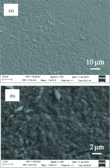
The SEM image and EDS characterization of a sulfured CZTS thin film are shown in Figure 1 and Table 1, respectively. The surface of the sulfured film is uniform and possesses several long particles. In order to determine what kind of particles were formed on the surface of the CZTS films, EDS analysis was used to check different area in a scale of 1 mm2. The EDS confirmed the atomic composition of each element. From the results shown in the table 1, Cu composition is a little low and the ratio of Cu/(Zn+Sn) is 0.69, where the Zn concentration is a little low with Zn/Sn ratio of 0.85. The ratio of S/metal is 1.01. The measure ratio of Cu:(Zn+Sn):S is 0.82:1.18:2, which is close to the stoichiometric CZTS formation represented as Cu2ZnSnS4.
 | Fig.1 SEM plane-view images of Cu2ZnSnS4 structure annealed film at different magnifications |
| Table 1 Compositional analysis of the typical CZTS sample sulfured at 550 ℃ |
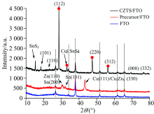
X-Ray diffraction (XRD) patterns of as-deposited and sulfurized CZTS films on FTO substrates are shown in Figure 2. The existence of elementary Cu, Zn, or Sn and several secondary phases were observed in the deposited films. The effect of sulfuring was distinctive in nature to obtain a better phase purity of electro deposited CZTS. The annealing was found to decrease all elementary phases of Cu, Zn and Sn as well as allotropes of sulfur. When the film was annealed at 550 ℃, the prominent (112), (220) and (312) peaks corresponding to crystalline phase of CZTS appeared. This film was purer, except for the coexistence of SnS2. The Three prominent peaks are located at 2θ =28.5° , 47.5° and 56.0° , respectively.
The size of CZTS crystals can be calculated using well known Scherrer equation.
 | Fig.2 XRD patterns of as-deposited and sulfurized CZTS sample on FTO at T=550 ℃ during 0.5 h |
Where D is the grain size, K=0.94, λ is the wavelength of Cu-Kα X-ray, β is the full width at half maximum of the selected peak, θ is the Bragg angle of the selected peak. The calculated crystalline size by Scherrer equation is between 35 and 45 nm.
However, in the XRD patterns, peaks corresponding to different phases may complicate and overlap the patterns. A complex peak appears as a broad one. Like these phases cannot be distinguished by XRD patterns. Because of this limitation, the phase identification in complex systems such as quaternary compound semiconductors may not be possible by XRD studies alone. Raman spectroscopy is often complementary to XRD techniques and has been included in the following subsection.
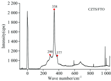
Raman spectra is commonly used to observe vibrational, rotational, and other low-frequency modes in a system to provide fingerprints of molecules. The main peak of CZTS sample located at 338 cm-1 with strong intensity was compared to other two lower peaks located at 290 and 377 cm-1 respectively, which is in agreement with other reported from kesterite CZTS. No Raman peaks for Cu2-xS and SnS2 with amode at 315 cm-1 were found. It means the content of SnS2 is very less. The two most intense peaks at 290 and 338 cm-1 assigned as the dominant non-polar A-symmetry modes, is consistent with earlier reports[26, 27, 28]. Raman peak at 377 cm-1 is identified with B-symmetry mode, while the peak at 366 cm-1 is identified with E-symmetry mode[29]. In general, the Raman spectroscopy agreed very well with the XRD measurement: the prepared CZTS film shows a strong phase of single chalcopyrite structure without much second phases.
In order to study the band gap of CZTS thin films, the optical properties of CZTS on FTO were measured via UV-Vis absorption spectroscopy. Figure 4 (a) shows the absorption coefficient (α ) as a function of wavelength or photon energy can be determined. The energy gap can be obtained using transmittance data from the absorption spectra by the following equation: Lambert-Beer Law.
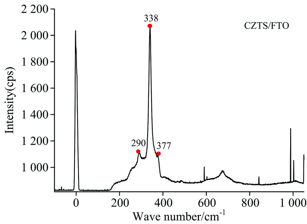 | Fig.3 Raman spectra of annealed CZTS sample in sulfur at T=550 ℃ |
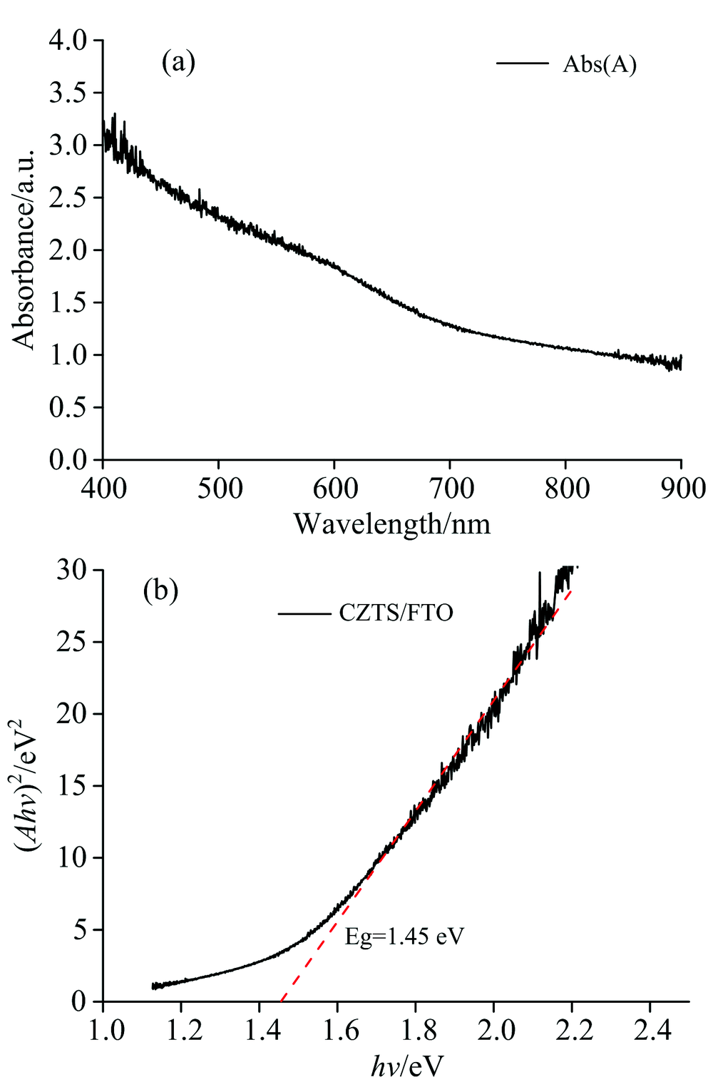 | Fig.4 (a) NIR-Vis absorption spectrum of CZTS films; (b) Plot of (α hν )2vs. photon energy (hν ) of the as re-crystallized CZTS |
Where α is absorption coefficient, Eg is the band gap and k is a constant. Extrapolation of a plot of (α hν ) vs. hν curve to zero, the calculated of Eg is about 1.45 eV, which is suitable for device fabrication.
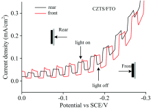
Figure 5 shows PEC performance of CZTS films (front and rear illumination) was investigated by linear sweep voltammetry (LSV) range 0 to -0.3 V. The big up climbing of photocurrent occurred when the CZTS film was illuminated under front/back irradiation. Upon switching to the dark, the photocurrent rapidly dropped. Photoelectrons transferred from conduction band of CZTS to the redox species through the interface of semiconductor electrode/electrolyte can be interpreted. Figure 5 also shows rear illumination caused a similar photocurrent density (0.18 mA· cm-2) compared with (0.16 mA· cm-2) front illumination at a biased potential of -0.2 V. And the voltammogram upon rear illumination was found to have lower photocurrent drop than front illumination after photocurrent reached the maximum height after illuminated. This result implicates that degradation might take place on the surface of CZTS film upon illumination. In general, light current is produced by FTO/CZTS under front/back irradiation, and the photocurrent flows in the same direction in both cases. This is a very promising result for bifacial solar cells.
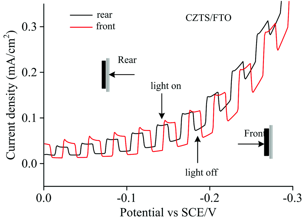 | Fig.5 PEC of CZTS on FTO conductive glass glass |
In summary, we prepared the Cu-Zn-Sn precursors by co-electrodeposition and obtained the CZTS thin film on the FTO coated SLG glass by a subsequent sulfuration process. The film surface is uniform and the elemental ratio is close to the stoichiometric CZTS formation. The synthesized CZTS films were characterized by various techniques such as scanning electron microscopy (SEM), X-ray diffraction and Raman spectroscopy. In this way, the structural, optical and electrical properties of CZTS films were investigated. The calculated optical band gap is about 1.45 eV. At last, PEC performance of the CZTS film were measured and compared for rear and font illumination. The results showed a great photocurrent density upon back and font illumination. These suggest the potential use of bifacial solar cells using transparent conducting substrates.
| [1] |
|
| [2] |
|
| [3] |
|
| [4] |
|
| [5] |
|
| [6] |
|
| [7] |
|
| [8] |
|
| [9] |
|
| [10] |
|
| [11] |
|
| [12] |
|
| [13] |
|
| [14] |
|
| [15] |
|
| [16] |
|
| [17] |
|
| [18] |
|
| [19] |
|
| [20] |
|
| [21] |
|
| [22] |
|
| [23] |
|
| [24] |
|
| [25] |
|
| [26] |
|
| [27] |
|
| [28] |
|
| [29] |
|