


硅基纳米柱GaN-LED的制备与光谱特性分析
[张雨茜 , 陆志成, 张伟, 郭俊宏, 张雪花, 胡芳仁
* ]
, 陆志成, 张伟, 郭俊宏, 张雪花, 胡芳仁]
|
|


作者简介: 张雨茜, 1994年生, 南京邮电大学电子与光学工程学院硕士研究生 e-mail: 18351922382@163.com
Ⅲ-Ⅴ族氮化物发光二极管因具有寿命长、 尺寸小、 高效、 节能等优点, 得到广泛的研究与应用。 随着光通信、 万物互联等领域的进一步发展, 需要开发高质量的微纳光源和微纳光波导。 纳米柱氮化镓发光二级管(GaN-LED)是一种重要的微纳光源, 具有广阔的应用前景。 另一方面, 作为应用最广的硅半导体材料本身并不是直接半导体, 发光效率低下而不能作为光源使用。 因此, 研究基于硅基板的纳米柱GaN-LED微纳光源具有非常重要的意义。 采用射频分子束外延技术(MBE)在Si基板上沉积并生长具有GaN缓冲层、 Si掺杂的n-GaN层、 4个周期的InGaN/GaN量子阱层和Mg掺杂的p-GaN层的GaN基PN结构。 利用扫描电子显微镜(SEM)观察其表面和侧面形貌, 可观察到以一定的倾斜角度生长于衬底表面、 排列紧密且整齐的纳米柱。 利用微纳加工技术制备纳米柱GaN-LED, 对已获得的纳米柱外延片进行SOG填充、 FAB刻蚀, 在p-GaN层和Si衬底侧蒸镀电极, 并对LED两电极施加直流电压, 进行I/V曲线和电致发光(EL)特性的测试。 纳米柱GaN-LED的阈值电压为1.5 V, 在室温下的峰值波长为433 nm。 纳米柱结构可有效减小LED的阈值, 在相同电压情况下, 纳米柱LED的亮度更高, 展现了良好的发光特性。 GaN纳米材料与体材料相比, 纳米结构中存在应力弛豫可以有效地降低位错密度, 尺寸小于光生载流子或激子的扩散长度, 因而能够减小光电子器件激活层中的局域化效应。 通过TCAD仿真, 对与实验结构相同的纳米柱GaN-LED两电极分别施加5, 6和7 V的电压, 可得到纳米柱LED的发光光谱。 仿真结果显示纳米柱GaN-LED的发光波长在414~478 nm之间, 发光颜色为天青蓝到蓝紫色之间, 峰值波长为442 nm, 发出鲜亮蓝色的光, 与实验获得的EL光谱结果相近。 随电压增大, 发光光谱峰值波长减小, 出现轻微的峰值波长蓝移。 在纳米柱结构中InGaN/GaN区域产生强烈的极化效应, 纳米柱结构在量子阱区域的载流子浓度增加, 削弱了量子限制斯塔克效应, 从而使LED波长峰值向高频率移动即蓝移。 其次, 纳米柱结构能够引起应力释放, 也会引起峰值波长蓝移。
Ⅲ-Ⅴ nitride GaN light emitting diodes (LEDs) have been widely studied and applied due to their long lifetime, small size, high efficiency and energy saving. With the further development in the fields of optical communication and interconnection, it is necessary to develop high quality micro-nano photonic sources and waveguides. Nano-column GaN-LED is an important micro-nano light source which has a broad application prospect. On the other hand, the silicon semiconductor material which is the most widely used is not a direct semiconductor itself, and its luminous efficiency is low and cannot be used as a light source. Therefore, it is very important to study nano-column GaN-LED micro/nano light sources based on silicon substrates. In this paper, a GaN buffer layer, a Si-doped n-GaN layer, a 4-period InGaN/GaN quantum wells layer and a Mg-doped p-GaN layer were deposited and grown on Si substrate by radio frequency molecular beam epitaxy technology(rf-MBE). The surface and side morphology of the nanostructures were observed by scanning electron microscope (SEM). Nano-columns which were grown on the surface of the substrate at a certain oblique angle and arranged closely and neatly can be observed. Nano-column GaN-LED was prepared by micro-nano processing technology. SOG filling and FAB etching were performed on the obtained nano-pillar epitaxial wafer, and electrodes were vapor-deposited on the p-GaN layer and S substrate side. DC voltage was applied to both electrodes of the LED. Photoelectric properties such as I-V curves and electroluminescence (EL) spectra were tested. The results show that the threshold voltage of nano-column GaN-LED is 1.5 V and the peak wavelength of nano-column GaN-LED is 433 nm at 290 K. The nano-column structure effectively reduces the LED threshold with smaller voltage. At the same voltage, the nano-column LED has a higher brightness and exhibits better light emission characteristics. Compared with bulk materials, the existence of stress relaxation in the nanostructures can effectively reduce the dislocation density. The size of the nanostructure is smaller than the diffusion length of photo-generated carriers or excitons, reducing the localization in the active layer of the optoelectronic device. By the TCAD simulation, the luminescence spectra of the nano-column LED can be obtained by applying voltages of 5, 6 and 7 V to the two electrodes of the nano-column GaN-LED respectively. The wavelength of nano-column GaN-LED is 414~478 nm. The luminous color covers from sky blue to blue-purple and the peak wavelength is 442 nm, which is close to the 433 nm of the EL. As voltage increases, the peak wavelength of the emission spectrum decreases, with a slight blue shift of the peak wavelength. In the nano-pillar structure, the InGaN/GaN region produces a strong polarization effect, and the nano-column structure increases the carrier concentration in the quantum wells region, which weakens the quantum-confined Stark effect, thereby shifting the peak wavelength of the LED to a high frequency which is called blue shift. Moreover, the nanopillar structure can cause stress release and also cause a blue shift in peak wavelength.
氮化镓(GaN)作为Ⅲ -Ⅴ 族氮化物半导体材料中的重要成员, 具有热导率高、 耐高温、 耐酸碱、 高硬度等优良的光学和电学性能。 通过改变不同含量的In, Ga和Al的氮化物具有从0.63~6.2 eV的连续禁带宽度, 可以用来制备紫外、 可见光以及光通信用发光器件。 而且, 基于GaN的发光器件具有寿命长、 尺寸小、 高效、 价格低廉、 轻便、 电光转化效率高、 节能以及易于集成等优点而得到广泛研究与开发应用。 目前国内外研究和市场开发的重点以平面结构氮化镓-发光二级管(GaN-LED)为主。 随着光通信、 万物互联等领域的进一步发展, 需要开发高质的微纳光源和微纳光波导。 纳米柱GaN-LED是一种重要的微纳光源, 具有广阔的应用前景。 另一方面, 作为应用最广的硅半导体材料本身并不是直接半导体, 发光效率低下而不能作为光源使用。 因此, 研究基于硅基板的纳米柱GaN-LED微纳光源具有非常重要的意义。
本实验采用分子束外延(molecular beam epitaxy, MBE)技术生长GaN纳米柱结构, 利用微纳加工技术制备纳米柱LED, 并对其光电性能进行测试表征和模拟仿真研究。
实验所用GaN纳米柱利用射频分子束外延设备(RF-MBE, Riber32)沉积而成。 在生长之前, 首先利用RCA标准工艺对Si基板进行清洗。 Si基底表面上附着有机物, 需要对Si衬底进行清洗。 分别用丙酮、 乙醇以及去离子水进行清洗。 丙酮很容易溶解基片表面的有机物, 同时使用超声波清洗仪可以清除附着的有机物。 最后用HNO3溶液和HF溶液对Si表面进行腐蚀清洗, 去除金属颗粒和氧化物层。
GaN纳米柱的生长过程: 首先将基板转移到高真空室内, 在850 ℃的条件下加热30 min除去衬底表面的残余氧化层。 随后将Si衬底温度降至680 ℃, 进行基板氮化。 然后在低温400 ℃生长一层50 nm厚的GaN缓冲层, 在高温840 ℃下生长1.3 μ m厚的Si掺杂的n-GaN层。 在590 ℃, 生长4个周期的InGaN/GaN量子阱层, InGaN厚度为3 nm, GaN的厚度为10 nm。 最后在600 ℃下生长60 nm厚的Mg掺杂的p-GaN层。
采用微纳加工技术制备硅基GaN纳米柱LED。 制备的工艺制作流程如图1所示。 首先在真空条件下将旋涂玻璃(spin on glass, SOG)填充到相邻纳米柱的间隙中, 然后使用快原子束(fast atom beam, FAB)轰击法去除p型GaN层上多余的SOG涂层。 并在Si的反面沉积300 nm厚的Al电极, 在p型GaN层上蒸镀20 nm的Pt和100 nm的Au, 得到完整而连续的n电极和p电极。
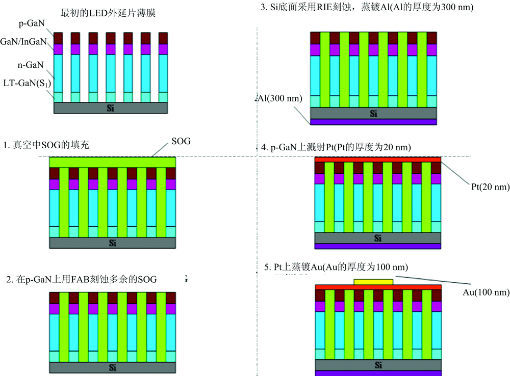 | 图1 纳米柱GaN-LED微纳加工制备过程Fig.1 Micro-nano fabrication process of the nano-column GaN-LED |
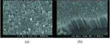
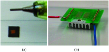
图2是扫描电子显微镜(SEM)下GaN基纳米柱的表面和侧面的照片。 每个纳米柱都以一定的倾斜角度生长于衬底表面。 相邻纳米柱之间虽然有空隙, 但是排列紧密且整齐。 纳米柱的直径分布在80~160 nm之间, 柱高为1.5 μ m。 从图中看出, 纳米柱生长并非十分均匀, 主要原因是硅衬底表面不平整, 有纳米级的起伏, 导致纳米柱的生长初期的成核不均匀, 以及生长工艺条件不稳定从而导致纳米柱的生长不均匀。 图3是制备好的纳米柱GaN-LED芯片。 对LED两电极施加直流电压, 便可进行I/V曲线和电致发光(electro luminescence, EL)特性的测试。 同时, 利用激光拉曼光谱仪测试其光致发光特性(photo luminescence, PL)。
 | 图2 GaN纳米柱的SEM图像 (a): 表面; (b): 侧面Fig.2 SEM images of the GaN nanocolumns (a): Surface; (b): Side |
 | 图3 纳米柱GaN-LED芯片的照片 (a): 制备的GaN-LED; (b): 粘贴在铝导热片上的GaN-LEDFig.3 Photos of nano-pillar GaN-LED chips (a): Photo of the prepared GaN-LED pad; (b): Photo of the GaN-LED pasted on aluminum therrnal |
图4是纳米柱GaN-LED的I-V特性曲线。 从测量结果可看出, 电压在0.5 V以前几乎没有电流, 电压一超过1.5 V, LED电流随电压增加迅速增大, 并开始发光。 该纳米柱GaN-LED的阈值电压大概为1.5 V。 根据资料显示, 平面结构的GaN-LED的阈值一般在2~3 V之间[1], 纳米柱结构有效的减小了LED的阈值, 施加更小的电压便可使LED发光。 当施加3V的电压时, LED的工作电流为11 mA。
 | 图4 纳米柱GaN-LED的I-V特性Fig.4 I-V characteristics of the nano-pillar GaN-LED |
GaN纳米柱结构基本上无位错, 可有效降低器件有源区内的缺陷密度, LED上的非辐射复合受到极大的抑制, 有源区中具有更少的漏电通道[2, 3, 4], 从而纳米柱LED 的漏电流更小, 因此纳米柱结构的LED阈值更低[5]。
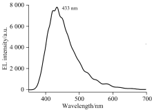
图5展示了纳米柱GaN-LED在室温下的EL光谱。 根据光谱图可以看出, 纳米柱GaN-LED的EL谱的峰值波长为433 nm, 为蓝色光。 纳米柱GaN-LED的EL谱的峰值半高宽(FWHM)为75 nm, 在材料生长过程中, 量子阱中InGaN层在降温过程中会出现In的局部聚集现象, 从而产生In的分布不均衡, 导致EL谱的FWHM展宽和驼峰。 采用MBE工艺生长的InGaN的EL谱的峰值半高宽一般比采用MOCVD工艺生长的InGaN的EL谱峰值半高宽要大些。
 | 图5 纳米柱GaN-LED的EL谱Fig.5 Electroluminescence (EL) spectrum of the nano-pillar GaN-LED |
利用Silvaco半导体工艺模拟及器件模拟工具(technology computer aided design, TCAD)软件中的Atlas器件仿真模块对纳米柱GaN-LED进行性能仿真。 仿真结构与实验的纳米柱GaN-LED的结构相同。 对纳米柱GaN-LED两电极分别施加5, 6和7 V的电压, 可得到纳米柱LED的发光光谱。 如图6所示。
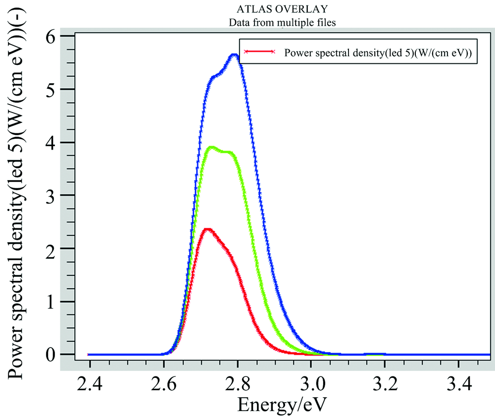 | 图6 外加5, 6和7 V电压的LED发光光谱Fig.6 LED emission spectrum with voltages of 5, 6 and 7 V |
由仿真图发现, 纳米柱GaN-LED的发光波长在414~478 nm之间, 发光颜色为天青蓝到蓝紫色之间, 在外加电压为7 V时, 峰值波长约为442 nm, 发出鲜亮蓝色的光。 与实验获得的纳米柱GaN-LED的EL谱曲线相似, 峰值波长较为接近。 随电压增大, 发光光谱峰波长减小, 出现轻微的峰值蓝移。 这是因为, 在纳米柱结构中InGaN/GaN区域产生强烈的极化效应, 在高注入条件下, 载流子在导带内的弛豫时间比载流子寿命要短很多[6, 7], 纳米柱结构在量子阱区域的载流子浓度增加, 屏蔽了部分内建电场, 削弱了量子限制斯塔克效应(QCSE), 从而使LED峰向高频率移动即蓝移[8, 9]。 其次, 纳米柱结构能够引起应力释放, 也会引起峰蓝移[10]。
采用分子束外延技术(MBE)生长包含4个周期InGaN/GaN量子阱的GaN基PN结外延片, 用扫描电子显微镜(SEM)观察到紧密整齐的纳米柱阵列, 利用微纳加工技术制备硅基GaN纳米柱LED。 然后对制备出的LED两电极施加直流电压, 进行I/V曲线和电致发光(EL)特性的测试。 纳米柱GaN-LED的阈值电压为1.5 V, 低于平面结构LED的阈值电压。 纳米柱GaN-LED电致发光EL谱的峰波长为433 nm, 与仿真所获得的电致发光光谱曲线相似, 峰值波长接近。
| [1] |
|
| [2] |
|
| [3] |
|
| [4] |
|
| [5] |
|
| [6] |
|
| [7] |
|
| [8] |
|
| [9] |
|
| [10] |
|