


介质阻挡放电系统复合气隙中三种放电丝的光谱研究
[孙浩洋1, 2  , 董丽芳
, 董丽芳1, 2, * , 韩蓉1, 2 , 刘彬彬1, 2 , 杜天1, 2 , 郝芳1, 2 ]
, 董丽芳, 韩蓉|
|


作者简介: 孙浩洋, 1993年生, 河北大学物理科学与技术学院硕士研究生 E-mail: sunhaoy@outlook.com
介质阻挡放电系统(DBD)作为一个典型的非平衡气体放电系统, 不仅在工业生产如低温等离子体生产和发光等方面被广泛应用, 而且该系统表现出的非线性现象、 自组织现象也吸引人们的关注。 DBD系统中放电丝的等离子体参量受诸多因素影响, 为了探究DBD系统的放电条件对等离子体参量的影响, 该实验重新设计放电单元以保证在其他实验条件相同的情况下, 对放电气隙间距和气体组分与等离子体参数之间的关系展开研究。 本实验的放电单元为一个平板型玻璃框架气隙, 该气隙由三个厚度均为1.2 mm, 放电区域边长分别为40, 30和20 mm的正方形玻璃框架复合而成, 因此该放电气隙有三个放电区域, 将此复合气隙放置于可调节气体成分和压强的真空室内, 可以同时产生三种放电气隙间距分别为1.2, 2.4和3.6 mm的等离子体放电丝。 高速录像机拍摄的瞬时照片表明三种放电丝均为随机放电丝, 即其放电类型均为流光放电。 在垂直于放电气隙平面的方向设置光路, 使用聚焦透镜获得清晰的成像, 移动光纤探头实现空间分辨并采集数据。 实验用光谱仪采集三种等离子体的氮分子第二正带系( C3 Πu→ B3 Πu) 谱线, 根据谱线强度计算得到各类放电丝的分子振动温度; 利用谱线中包含的氮分子离子
Dielectric barrier discharge system (DBD) is a typical nonlinear gas discharge system, which not only has many applications in the industrial production such as low temperature plasma production and luminescence, but also has attracted widespread attention for its physical phenomenon such as non-linear phenomenon and self-organization phenomenon. In order to study the influence of gap distance and gas components on plasma parameters of discharge filaments in DBD system, a discharge cell is redesigned to ensure the other experiment conditions are the same. The discharge cell of this experiment is a flat multiplicate gas gap, which is composed of three thickness of 1.2 mm square glass frames with the discharge area side length as 40, 30 and 20 mm respectively. The multiplicate gas gap is placed in a vacuum chamber with adjustable gas composition and pressure, and three discharge filaments can be generated whose discharge gap distance is 1.2, 2.4 and 3.6 mm respectively. The instantaneous photos taken by high speed video camera indicate that the discharge types of three filaments are all streamer discharge. Arranging the optical path on the line perpendicular to the plane of gap, the focus lens is used to obtain a clear image, and optical fiber probe is moved to achieve spatial resolution acquisition data. The emission spectra of the N2 second positive band ( C3 Πu→ B3 Πu) of the three filaments are collected in the experiment by spectrograph. The molecule vibration temperatures are calculated based on emission intensity; based on the relative intensity of the
介质阻挡放电(DBD)是典型的非平衡气体放电系统[1], 其装置简单, 操作便捷, 可以在大气压下低成本的产生低温等离子体, 因此在等离子体灭菌消毒[2], 等离子体化学气相沉淀 (PECVD)[3], 等离子体发光显示[4, 5]等工业领域有着广泛的应用。 为了合理地调控DBD系统中的放电, 使其达到最佳的放电效果, 探究实验条件对放电丝等离子体参数的影响是很有必要的。
本实验在原实验装置上进行改变[6], 同一气隙中有三个放电区域, 可以同时产生三种不同的放电丝, 在电压U、 交流频率f、 气室气压p保持不变的实验条件下研究这三种等离子体的分子振动温度和电子平均能量随气隙间距d值的变化, 通过改变氩气含量得到了分子振动温度和电子平均能量的变化规律。
实验核心装置如图1所示, 电极由两个内部装满水的圆柱形容器组成, 两侧由1.2 mm厚度的玻璃密封作为电介质板, 水电极内部各有一个金属环浸入水中并与高压高频交流电源连接。 两个水电极之间固定着特制的玻璃框架, 此玻璃框架由三个厚度均为1.2 mm, 边长分别为20, 30和40 mm的正方形框架复合成一个放电气隙。 因此该气隙分为A, B和C三个放电区域, 三个区域的气隙间距分别是dA=1.2 mm, dB=2.4 mm, dC=3.6 mm。 电压电流信息由高压探头(Tektronix P6015A)连接至示波器(Tektronix DPO 4104B)记录。 整个电极部分放置在气压和气体组分可调节的密闭真空室内, 通过真空室的进气孔和排气孔可以改变气室内气体组分。
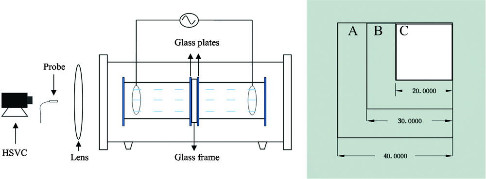 | 图1 实验装置图及放电气隙主视图Fig.1 Schematic diagram of the experimental setup and main view of the gap |
在垂直于介质板平面的直线上布置光路, 使用焦距为175 mm的聚焦透镜将放电丝成像, 放电丝与透镜之间的距离(物距)约为25 cm。 在成像平面移动光谱仪 (Acton Spectra Pro 2750, CCD: 1340 400 pixels, grating: 300, 1 800和2 400 grooves· mm-1)的光纤探头可以实现空间分辨采光, 即采集不同放电丝辐射的光, 并通过计算机程序处理, 计算。 通过透明观察窗可以用数码相机(Canon EOS 6D and Canon Macro 100 mm)和高速录像机 (HFVC; pco.dimax S4) 拍摄录制照片。
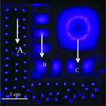
本实验在之前的实验装置基础上进行了创新改变, 实现了在一个放电气隙中同时产生三种放电丝, 三个放电区域的气隙间距分别为1.2, 2.4和3.6 mm。 放电气隙两侧与水电极紧密相接。 图2给出了同时产生的三种放电丝, 根据气隙间距分别记作A(dA=1.2 mm), B(dB=2.4 mm), C(dC=3.6 mm), 从照片可以看出三种放电丝在视觉上具有明显差别。 整个实验过程中外加电压U、 电源频率f、 气压p保持不变, 因此同气体组分中放电丝的等离子体参量只与不同放电区域的气隙间距有关; 改变气体组分得到各类放电丝等离子体参量的变化只与气体组分有关。
 | 图2 三个区域中产生的放电丝Fig.2 Three kinds of discharge filament The applied voltage U=2.8 kV; the driven frequency f=55.5 kHz; gas pressure p=18 kPa; the gas gap A: 1.2 mm, B: 2.4 mm, C: 3.6 mm. The exposure time: 25 ms |
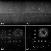
图2中的照片曝光时间为25 ms, 是上千次放电的叠加效果, 为了从更高的时间分辨率上观察这些放电丝, 我们使用高速录像机在不同曝光时间下拍摄了一系列照片。 如图3所示, 这些照片曝光时间分别为10, 20, 100和500 μ s, 即半周期、 单周期、 多周期和多周期。 可以看到三种放电丝A, B和C均为随机放电丝, 随着曝光时间的增加, 成像越来越清晰明亮并且接近人眼视觉和普通数码相机的拍摄效果, 这说明三种放电丝本质上都是DBD中的流光放电。
 | 图3 不同曝光时间下的高速录像机照片Fig.3 Images taken by high speed video camera with different exposure time (a): 10 μ s; (b): 20 μ s; (c): 100 μ s; (d): 500 μ s |
为了研究三种放电丝的等离子体状态和参数, 实验中选用300 grooves· mm-1的光栅, 设定中心波长为390 nm, 采集波长范围为360~420 nm的氮分子第二正带系(C3Π u→ B3Π u) 的发射谱线。 如图4所示, 根据氮分子第二正带系的两组振动序带: Δ ν =-2 (0-2, 1-3, 2-4) 和Δ ν =-3 (0-3, 1-4, 2-5) 的发射谱线强度进行处理和计算, 得到放电丝的分子振动温度[7]。
 | 图4 360~420 nm范围内的发射光谱Fig.4 Emission spectra in the range of 360~420 nm |
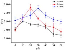
图5给出了三种放电丝的分子振动温度随混合气体中氩气含量的变化关系, 误差棒是多次测量和计算结果的标准差。 可以发现, 三种放电丝在纯空气条件下的分子振动温度较低, 随着氩气含量增加分子振动温度会达到一个峰值然后再降低。 不同气隙厚度中的放电丝的分子振动温度出现峰值的位置不同, 放电丝C最先达到峰值, 放电丝B在氩气含量20%左右达到峰值, 放电丝A在氩气含量30%左右达到峰值。 从总体趋势来看, 同氩气含量下, 放电丝分子振动温度在1.2 mm气隙间距中最高, 2.4 mm气隙间距次之, 3.6 mm气隙间距中的最低。
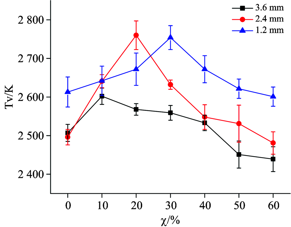 | 图5 三种放电丝的分子振动温度随氩气含量的变化Fig.5 Variations of molecule vibrational temperature of the discharge filaments in different area as a function of Ar concentration |
DBD系统中电子在电场加速的作用下获得能量并撞击分子, 分子受撞击后获得能量并向低能级跃迁, 此过程会辐射出光子。 电子能量大多数在10 eV以下, 但是也会有一些电子能量可以达到分子离化阈值。 在实验中, 除了采集到氮分子第二正带系谱线外, 还采集了氮分子离子
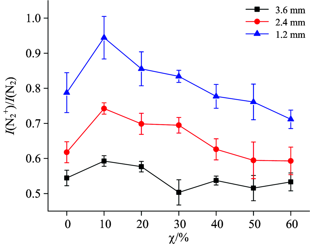 | 图6 三种放电丝的电子平均能量随氩气含量的变化Fig.6 Variations of electron average energy of the discharge filaments in different area as a function of Ar concentration |
实验通过三层气隙复合介质阻挡放电装置, 首次在同一放电气隙中研究了放电气隙间距d和氩气含量对同时产生的三种放电丝的影响, 排除了其他实验条件对实验的影响。 通过发射光谱法对同时产生的三种放电丝进行光谱诊断, 并研究放电丝的分子振动温度和电子平均能量。 结果表明, 随着氩气含量的增加, 三种放电丝的分子振动温度均会先升高再降低, 并且出现峰值时的氩气含量略有不同; 整体来看, 同样氩气含量条件下, 1.2 mm气隙间距中的放电丝分子振动温度最高, 2.4 mm气隙间距次之, 3.6 mm气隙间距的最低。 三种放电丝的电子平均能量均在氩气含量为10%左右达到峰值, 随着氩气含量的增加, 电子平均能量均降低, 且1.2 mm气隙间距下降最快, 3.6 mm气隙间距下降最慢; 在氩气含量相同的情况下, 1.2 mm气隙间距中放电丝电子平均能量最高, 2.4 mm气隙间距的次之, 3.6 mm气隙间距中的最低。 实验所得结果对DBD系统中等离子体参量研究和工业生产具有重要参考意义。
The authors have declared that no competing interests exist.
| [1] |
|
| [2] |
|
| [3] |
|
| [4] |
|
| [5] |
|
| [6] |
|
| [7] |
|